Diodes evaluation for crystal
sets, a simple practical approach
by SV3ORA
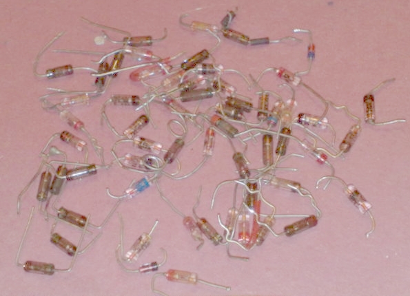
Recently, I had the chance to own a bunch of germanium diodes. This was the kick-start to begin an experiment for evaluating sensitivity of different types of germanium point contact diodes, for use in the crystal sets.
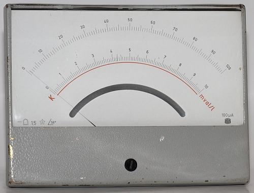
The experiment was simple. I connected a very sensitive current meter, shown below, to the germanium test diode and to the ground. On the other end, the diode was connected to a few turns of wire, forming an air coil of about 1cm in diameter. The other end of the coil was connected to the ground.
The test transmitter was a 446MHz PMR placed about 30-40cm away from the coil. For the experiment, I was standing exactly in the same place each time I turned on the transmitter, as even the slightest movement affects the reading on the meter.
From the 11 types of germanium detector diodes I tested, the winners were:
1. OA90, reading current >100uA
2. AA119 and OA47, reading current >100uA, just a little bit lower than the
OA90.
3. AA143, reading current >85uA
To give you an indication of the sensitivity, with the same setup, a 1N34A reads only about 20uA.
I have also tested two of my best unmarked diodes and they read the same as AA119. These unknown diodes were tested before on a real crystal set and gave the best sensitivity, thus I assume my readings are quite ok, despite the much higher frequency used. Although, I did not test the diodes for different input power levels.
References: Information from different websites about diodes used as detectors
Website 1
Diodes comparison
All of the diode
detectors described above have at least one diode forward voltage-drop
in the path to the measuring device. The diode forward voltage drop, Vf,
varies approximately in proportion to the logarithm of the current, If,
passing through the diode, and also depends on the temperature of the
diode junction. For many types of diode, this behavior is described to a
good approximation by a modified form of the Ebers-Moll equation:
where k is Boltzmann's constant
(1.380662´10 |
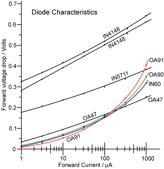
| The 1N4148 is a silicon
P-N junction diode. The 1N5711 is a silicon Schottky diode. The OA47 is
an archaic germanium gold-bonded diode, and the rest are germanium
point-contact diodes. Two 1N4148 diodes from different manufacturers
were measured merely to illustrate the point that silicon P-N diodes
have the highest forward voltage drop and are therefore a poor choice
for low voltage detectors. The 1N5711 curve is the average of results
from four diodes, all from the same batch, which had practically
identical characteristics. The OA47 curve is the average for four diodes
from two manufacturers, all having similar characteristics. The OA90,
OA91, and 1N60 curves are from single examples, and are therefore not
necessarily representative of the type. All data were recorded at an
ambient temperature of 21°C. The data indicate that the IN4148, the 1N5711, and the OA47, all obey a logarithmic V/I relationship rather well, whereas the germanium point-contact characteristics show considerable curvature due to high internal resistance. With regard to the forward drop however, the germanium diodes are all superior to the IN5711 in the 1-100mA range, and the preference for the latter may merely reflect the fact that many semiconductor manufacturers can no longer fabricate germanium. Silicon Schottky diodes, such as the 1N5711 and 1N6263, being essentially UHF devices, have better high-frequency performance than germanium diodes, but germanium diodes work well at VHF and are therefore perfectly adequate for HF applications. Among the germanium diodes, there is little difference between the gold-bonded and standard varieties in the 1 to 100mA range, but the OA47 is the best choice for currents up to 1mA. We should observe however, that detector diodes only conduct on the peaks of the applied waveform, and so the instantaneous current is much higher than the average current, the difference being about an order of magnitude. Therefore, in selecting diodes for average currents in the region of 1 - 100mA, we should consider the steady-state voltage drop in the region 10mA - 1mA; in which case the germanium gold-bonded diode offers the lowest forward-drop without contest. Note however, that one of the consequences of the Ebers-Moll equation is that low forward voltage-drop is associated with high reverse leakage current. If reverse leakage is an issue, then silicon Schottky diodes are to be preferred. To put this issue in perspective however, the reverse leakage current of an OA47 diode was measured as follows: |
| |
|
|
|
|
|
|
|
| |
|
|
|
|
|
|
|
| The leakage current is approximately linear in the 5-20V range and may be modelled by assuming a resistor of about 2MW in parallel with the diode. Such a defect has little effect on the operation of a detector loaded with a 10-100KW resistor. Some final points in favour of the silicon Schottky diodes however, are that germanium diodes show a wider spread of characteristics, and that the OA47 is obsolescent. Hence the Schottky diodes are definitely preferable in applications requiring diode matching, precise calibration, or availability through normal commercial channels. The 1N5711 in particular also, has a very high reverse breakdown voltage for a device of its class, its Vr max of 70V making it suitable for half-wave detectors of up to 24.7V DC ouput. An OA47 half-wave detector has a maximum DC output of 10.6V if Vr max is not to be exceeded. |
| Detector diode data: |
| Type | Description | / V |
/ mA |
/ mA |
|
|
||
| |
|
|
|
|||||
| 1N5711 | Si Schottky (2.0pF) | |
|
|
|
|
|
|
| 1N5712 | Si Schottky (1.2pF) | |
|
|
|
|
|
|
| AA119 | Ge point contact | |
|
|
|
|
|
|
| AAY30 | Ge Au-bonded. High speed | |
|
|
|
|
|
|
| AAY32 | Ge Au-bonded. High speed | |
|
|
|
|
|
|
| AAY33 | Ge Au-bonded. High speed | |
|
|
|
|
|
|
| AAZ15 | Ge Au-bonded. High voltage | |
|
|
|
|
|
|
| AAZ17 | Ge Au-bonded. Gen.purpose | |
|
|
|
|
|
|
| BAT81 | Si Schottky (1.6pF) | |
|
|
0.41 1.0 |
1 15 |
|
|
| BAT82 | |
|||||||
| BAT83 | |
|||||||
| OA47 | Ge Au-bonded. Gen.purpose | |
|
|
|
|
|
|
| OA90 | Ge point contact "diode"?** | |
|
|
|
|
|
|
| OA91 | Ge point contact | |
|
|
|
|
|
|
| OA95 | Ge point contact | |
|
|
|
|
|
|
| * max. ** a very non-linear resistor pretending to be a diode - best avoided! |
For the Omega receiver I have decided to go for
the OA47 diode, based on it's obvious advantages over the other diodes. The
second generation of the receiver may use a FET detector, but I first have to
make a better research on this type of detector. So, for the time being, and to
satisfy more classical set readers I will end up to this type of diode.
| Back Diodes: One further rectifying device which we should mention in passing is the backward diode or 'back-diode'. This is a special type of tunnel diode (Esaki diode), which has an extremely low forward voltage drop: in the region of 90mV for 10mA forward current. Unfortunately however, there is no get-out-of-jail-free card as far as the Ebers-Moll equation is concerned: the back diode has an extremely low reverse breakdown voltage, and a leakage of around 1mA for a mere 500mV of reverse bias. The back diode can therefore only be used in extremely low-impedance low-voltage circuits, which comprehensively defeats any advantage it might have had for the construction of linear detectors. |
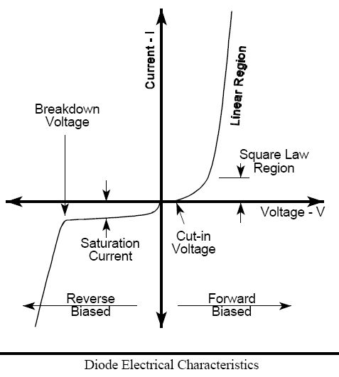
Below I would like to mention two useful things about diodes. The detected voltage as function of the input voltage and the detector diode input impedance
| Detected voltage as
function of the input voltage If we rectify a RF signal with a diode we can distinguish two situations. Situation 1: Rectifying in the linear region If the input voltage is high enough (well above the voltage drop of the diode at 1 mA), the output voltage of the diode will be about proportional to the input voltage. So double input voltage, gives about double output voltage. The output voltage is almost equal to the peak value of the input voltage. The power losses in the diode are in this region very low compared to the rectified power. Situation 2: Recifying in the square law region If the input voltage is low, lower then the voltage drop of the diode (at 1 mA) then the situation is completely different. The input of the diode behaves for the RF signal like a resistor with value RD. The output of the diode behaves like a DC voltage source in series with a resistor, the value of this resistor is also equal to RD. The value of the DC voltage source is square law related to the amplitude of the RF input signal. So double input voltage, gives 4 times as much detected DC voltage at the output In the square law region the output voltage of the diode will be much lower then the input voltage, the diode gives much power loss between input and output. The lower the input voltage, the higher the losses. The higher the input voltage, the lower the diode losses. When further increasing the diode input voltage, we gradually come into the linear detection region. When receiving weak stations, detection takes place in the square law region. Between the linear and square law region, there is a region not linear, and not square law but somewhere in between.
|
| Detector diode
input impedance A point to which we have so-far only alluded, is that the load presented by the detector has a significant effect on the operation of some types of bridge. We must therefore always keep the detector input impedance in mind when investigating bridge behaviour, and in order to do so we need to have an idea of its value. This is a peculiar problem in the case of a diode detector, because the diode does not obey Ohm's law; and so the input resistance varies during the course of each cycle of the applied voltage. For the most part however, it is sufficient to have an average picture of the detector input impedance, and this can be obtained by considering the power delivered to the detector load resistor RD. |
| In the first instance, we
can consider the power delivered to RD in the limit that the peak value
of the applied voltage Vdet is very large in comparison to the diode
forward voltage drop Vf. In this case, the detector output voltage is: Vmeas = Vdet Ö2 and the power delivered to the load resistor is: Pdet = Vmeas˛ / RD |
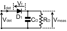 |
| Now, all of this power
must come from the bridge output. Therefore, if we define the detector
input resistance as Rdet, we have: Pdet = Vdet˛ / Rdet = Vmeas˛ / RD and using equation (Vmeas = Vdet Ö2) gives: Vdet˛ / Rdet = (Vdet Ö2)˛ / RD i.e., 1 / Rdet = 2 / RD i.e.,
Thus the limiting input resistance of a
simple detector is equal to half the detector load resistance. We
can understand this point by thinking of the detector as a kind of
voltage transformer. The RMS average of a DC signal is the same as its
ordinary average, and so in the process of converting from AC to DC, the
RMS level has been transformed-up by a factor of Ö2. Thus the detector
is a 1:Ö2 voltage transformer, and hence a 1:(Ö2)˛, i.e., 1:2 impedance
transformer.
Thus the voltage-doubler is a limiting
1:8 impedance transformer. Consequently, it has a much lower input
resistance in comparison to a non-multiplying detector for a given value
of detector load. The difference is such that advantage of increased
output voltage can easily be lost as a result of loading of the driving
circuit. |
Website 2
 For smaller signals, the diode forward voltage (0.6v for silicon, 0.3v for
germanium or schottky) causes error: output DC voltage is lower than peak RF
voltage. And any diode no longer has a well-defined delineation between
conduction and non-conduction for small signals: its rectifying properties
become inefficient. Signal levels between a few volts down to a few tens of
millivolts require some significant non-linear corrections to be factored in.
Detectors such as thermocouples or thermistors (bolometers) can do a better job
in this region. We tend to dismiss diodes as error-prone for small signal
measurements.
For smaller signals, the diode forward voltage (0.6v for silicon, 0.3v for
germanium or schottky) causes error: output DC voltage is lower than peak RF
voltage. And any diode no longer has a well-defined delineation between
conduction and non-conduction for small signals: its rectifying properties
become inefficient. Signal levels between a few volts down to a few tens of
millivolts require some significant non-linear corrections to be factored in.
Detectors such as thermocouples or thermistors (bolometers) can do a better job
in this region. We tend to dismiss diodes as error-prone for small signal
measurements. 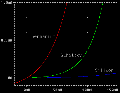 What diode to use? All diodes will follow the square-law rule for small signals.
We should choose one that is fast, so 1N4000-series power diodes are out. Any
diode with a lot of capacitance is out. Diodes with a sharp I vs. V curve will
give more output, so silicon diodes are less desirable. Schottky diodes are
great, but they require DC biasing to get into the really curved part of the I
vs.V curve. With zero bias, a germanium diode has very decent qualities (apart
from nasty temperature effects). When Hewlett Packard makes square-law diodes
using exotic semiconductors like gallium arsenide with molecular-beam-epitaxy
machines, the result looks remarkably similar to a simple point-contact
germanium diode like a 1N34A. Only repeatability and stability are much better -
they need to measure absolute voltage.
What diode to use? All diodes will follow the square-law rule for small signals.
We should choose one that is fast, so 1N4000-series power diodes are out. Any
diode with a lot of capacitance is out. Diodes with a sharp I vs. V curve will
give more output, so silicon diodes are less desirable. Schottky diodes are
great, but they require DC biasing to get into the really curved part of the I
vs.V curve. With zero bias, a germanium diode has very decent qualities (apart
from nasty temperature effects). When Hewlett Packard makes square-law diodes
using exotic semiconductors like gallium arsenide with molecular-beam-epitaxy
machines, the result looks remarkably similar to a simple point-contact
germanium diode like a 1N34A. Only repeatability and stability are much better -
they need to measure absolute voltage.