by SV3ORA
Presented by Juhász András at the The Budapest New Technology Meetup Group on July 4, 2012.
Some photos and his presentation can be found here.
My goal: To face the challenges occurring from building a simple transistorized 4-bit digital computer, made entirely out of discrete DTL, including the ROM and RAM. It should be made cheap and everything should be hand wired.
Don't ask why I am doing this.
Don't ask how much time is it going to take.
For detailed info on how the
computer works, see this
project. Here, I am only going to replicate this design on a discrete DTL
basis designed by me, providing all the necessary details required to build one. I am not going
to provide unnecessary details, such as the theory behind the gates
construction, as this could be quite time consuming. Nevertheless, going on
discrete gates, some changes have to be done in the original schematic in order
to work. Also some modifications and added features may be present in my design.
CURRENT PROJECT STATUS
New, simplified version of the
input/output (6-7-2012)
New, much simplified version of the programmer. (4-7-2012)
Front panel for the computer.
(11-6-2012)
New corrected version of the programmer. (11-6-2012)
New version of the programmer with
program write safety and indicator. (9-6-2012)
Punch card reader completed and
tested (27-5-2012)
Punch card reader construction completed
(25-5-2012)
Punch card reader design completed
(25-5-2012)
Punch card reader mechanical
construction completed (21-5-2012)
New version of programmer with
punch card reader inputs. (20-5-2012)
Input/output design completed.
(5-5-2012)
Programmer completed. (28-4-2012)
Accumulator and flags display part
of the programmer completed. (10-4-2012)
Data, instruction and display part
of the programmer completed. (5-3-2012)
Address and
display part of the programmer completed. (3-3-2012)
PROGRAMMER and DISPLAY
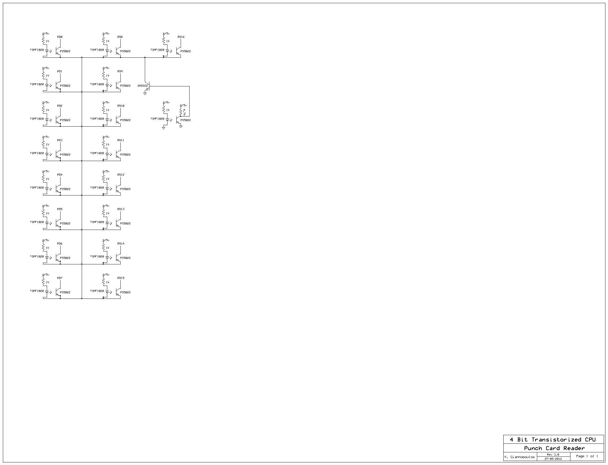
The main schematic of the programmer and display I have designed is shown below. Click on the picture for a bigger image.
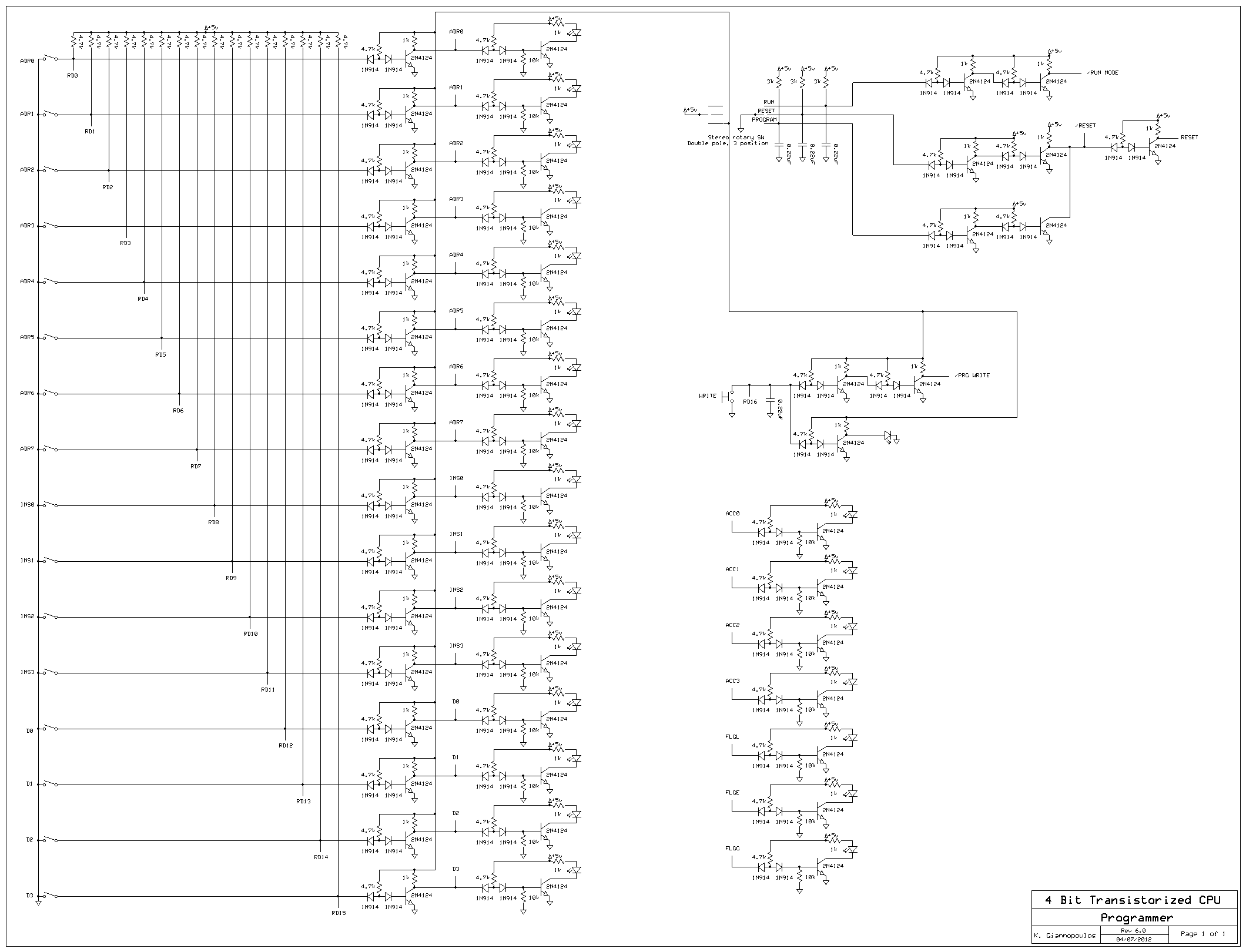
To save on gates, I have not used buffers to set the address, instruction and data bits, but just inverters. I have also found it more convenient to think of a closed switch as bit 1, rather than the opposite way round. This does not affect the operation of the rest of the computer.
In programmer version 1, a single inverter, switched on the power to a series of 16 transistor gates on the programmer. This transistor set the enable wire to either 0.6v (logic 0) or 5v (logic 1). The programmer in that version did not worked as expected, as there was probably a fan-out problem. The single inverter could not drive 16 gates directly, but a maximum of 3 of them.
To deal with the problem, I produced a second version of the programmer. I disconnected the enable wire from the transistor inverter and I replaced the mode multi switch with a stereo one. Each time program mode is selected, by one portion of the stereo switch, the other portion connects the 16 gates directly to vcc, therefore enabling them. Since there is no electronic connection of this enable wire to the rest of the computer, this simple mechanical trick works fine.
The only change in version 3, was the addition of inputs to support a punch card reader (RD0-RD16). In version 4, a simple modification at the PRG WRITE circuit, allowed protection from accidentally writing memory when in RESET and RUN mode. When not in PROGRAM mode, the output of the circuit is always floating, independent of the WRITE button state. This floating output is seen as logic one by the rest of the computer. A WRITE pulse indicator is added too, as this was thought to be helpful. In version 5, the 3k resistor at the WRITE pulse circuit has been removed, to allow for good card reader sensitivity. The card reader is now biased only from the base resistors of the WRITE pulse circuit. Logic one, will now be represented as a floating input and not as 5v. The result is identical.
The final version is 6. Thanks to Rory Mangles, the LED driving circuits have been simplified in a single transistor, significantly reducing the number of transistors used in the programmer. The drawback with this simpler approach is that the LEDs are not completely switched off on zero logic but they are very dim. To correct this, I have added a 10k resistor from the transistor base to the ground. Now everything works as expected.
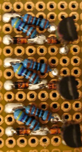
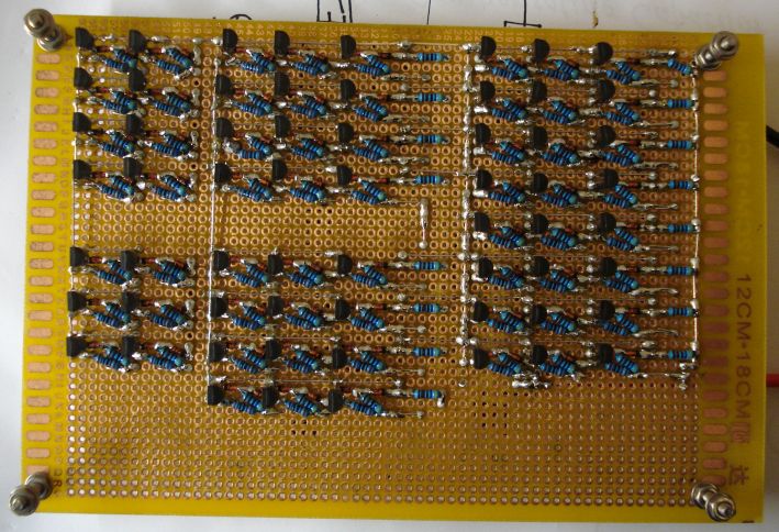
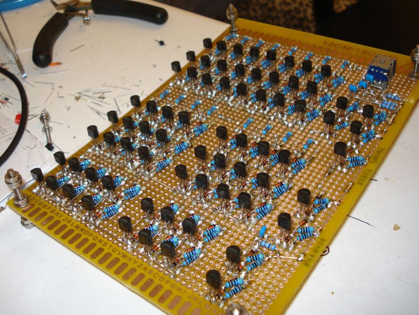
Below, a single inverter and how it is soldered on the proto board is shown. I have chosen a way to solder the components on the board that would be quick to solder and at the same time, consuming less space.
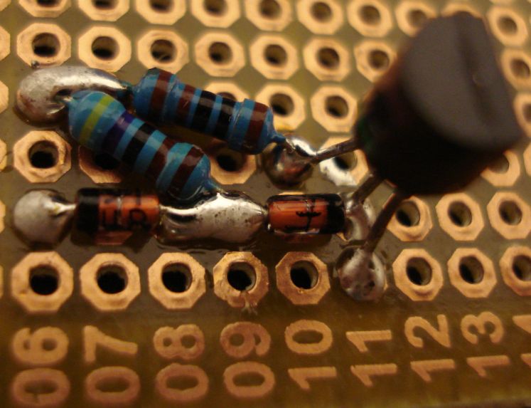
All the components and some wiring are soldered on the copper side. The rest of the wiring (mainly power supply lines), LEDs and pins, is done on the opposite side of the board. I found this way faster to solder and debug. Below, three inverters are stacked together (power supply lines are not present).
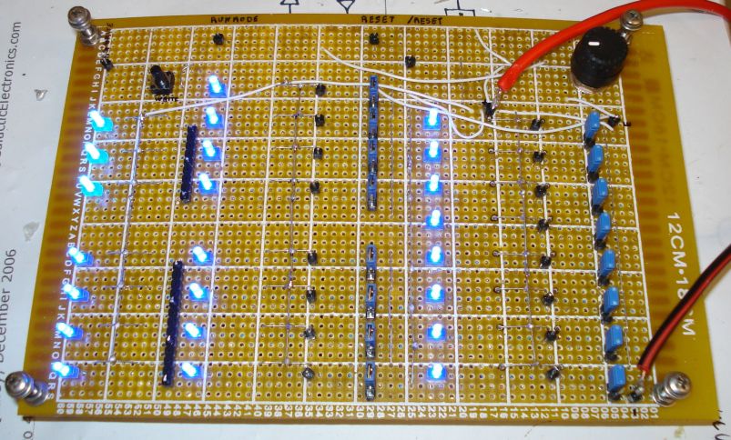
The 8-bit address and display section has been completed below. The circuit consumes 5V @ about 100mA.
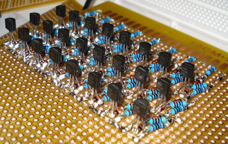
The bit settings are done using jumpers which are cheap and small. If a front panel is to be made, these jumpers can be very easily replaced by switches, fitted on the male pin rows using female pin rows or direct soldering.
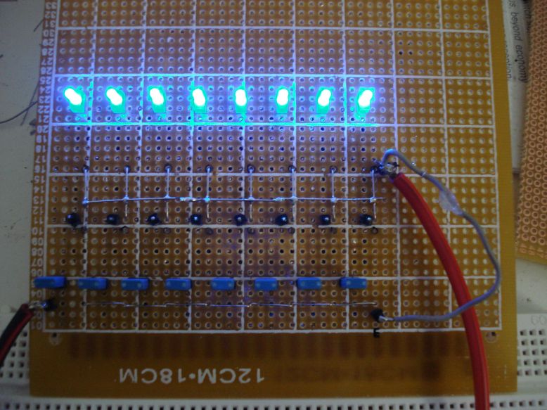
The data and instruction part and their display has been completed below.
Accumulator and flags display part of the programmer completed below
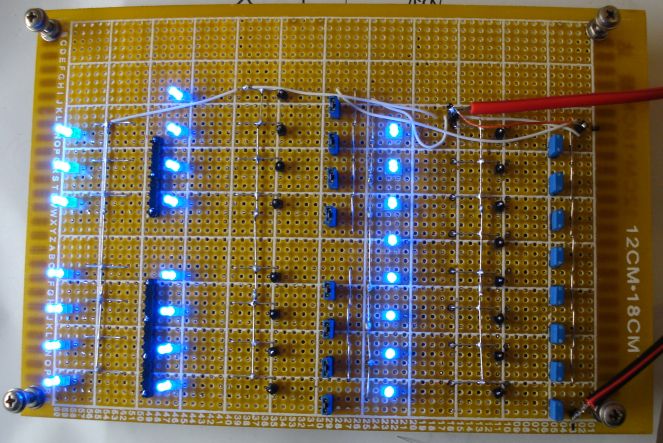
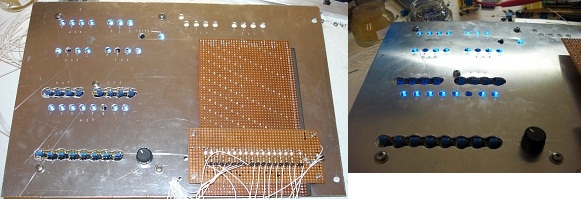
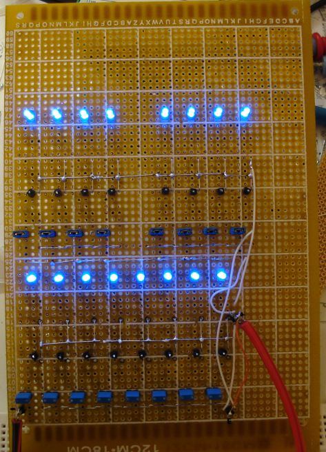
Programmer completed and tested!
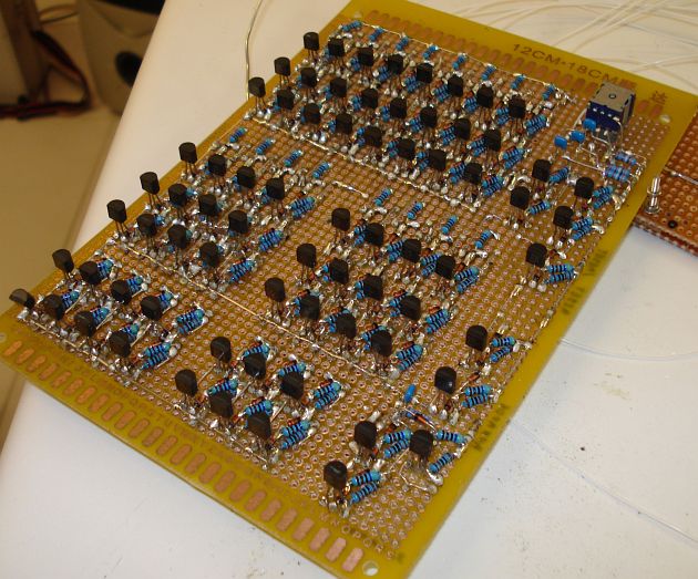
The programmer after the simplifications of the last version
PUNCH CARD READER
If you have written a program for the computer, programming it is a fairly easy process. But switching 16 switches to program just a single row in memory can be very time consuming in large programs. Therefore, I have decided to make a punched card reader, which allows rapid programming of the computer, within a few seconds.
Optical reading is the best choice for ensuring reading repeatability. You need 18 IR LEDs and 18 IR photo-transistors. 16 of them are for the data, address and instruction. The remaining 2 are for the WRITE pulse and the card auto detection. Try to find the smallest packages, in order to reduce the total card size, but do not solder them too close, as the IR light might affect adjacent sensors. I have left a one-hole space between most of the adjacent sensors in my reader, to ensure this.
Since the photo-transistors are connected in parallel with the programmer switches, you have to ensure that before inserting a card in the reader, all the programmer switches must be open (i.e. not connected to ground). This has to be done manually.
You also have to ensure that the reader won't interfere with the manual switches programming, when there is not card in it. For that purpose, the reader uses a mechanism to auto detect if a card has been inserted. The reader will enable itself as a programmer input, only when a punch card has been inserted into it. This is accomplished by a separate sensor that is mounted below others (right-bottom in the next picture), which enables the rest of the sensors, only after a card has been slipped through. Since the position of this sensor is below others (assuming the card slips-in from top to the bottom in the next picture), it will ensure that a card will be always present in the position of the rest of the sensors when they are enabled, therefore avoiding random data writing in memory positions. Also, you have to detect when the card has been slipped-out completely, in order to disable the reader again. The same detection mechanism is used like before, to accomplish this and a small cut on the card ensures this (more on this at the template card section).

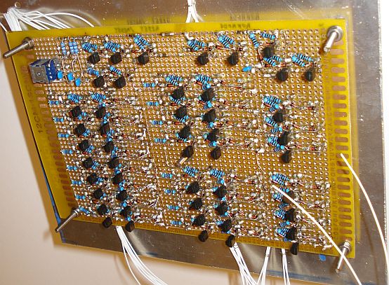
As far as concern the mechanical construction, the same prototype board material is used to make the punched card reader. This is a good choice as it is cheap an the holes have already been drilled and perfectly aligned.
You need to make the sensors/LEDs holes a bit larger, depending on the diameter of the ones you have available. The important bit, is to make the write-pulse hole quite smaller than the rest of the holes. This will ensure that all the other sensors will be set, when the write pulse is created. In my prototype, I left the proto-board hole as wide as it was, for the write-pulse sensor.
All sensors are mounted on the solder side of the proto-board, facing towards the non-solder side. If the sensors are quite small (smd sized), the holes of the board will act themselves like a small tube-like construction for each sensor, which further ensures no-interference from adjacent sensors.

Two proto boards are needed to make the punch card reader. The first, contains the IR LEDs and the second, the IR photo-transistors. These are sandwiched like shown in the next photo, with the sensors soldered on the solder sides (outwards) and faced towards the inner sides. Two small pieces of the same material, are inserted on both ends, to create the necessary spacing for the punch card that slips in and at the same time to ensure correct alignment of the punch card. In fact, a little more spacing is needed, to compensate for the punch card solder hole filling (filling the holes of a single sided proto card with solder, will create a small solder ball onto each hole) and this spacing is done by adding one washer on top of the spacing board pieces. The whole construction is held together firmly, using four small screws.
Making the punch card reader like this, ensures correct alignment of the punch card that slips-in. Slipping-in the punch card is not quite smooth and it usually requires more force. Nevertheless, this fact, minimizes the unwanted case of accidentally slipping the card backwards. Even if you have left a punch card inside the reader and you turn it upside down, the card won't slip-out backwards.
Punch card reader completed
Preliminary punch card reader test video
Punch card template
In order to ensure that the reader will only de enabled when there is a card slipped in and it will be disabled when the card is not present and at the same time to prevent accidental bits writing, the punch card template shown below must be made for each of your programs. Please click on the picture to see a description of the different areas on the punch card.

Using this card template, there is also the advantage that if a bigger program needs to be written you may split it in more than one cards and insert them in sequence.
With the existing reader configuration mentioned above, the write pulse holes on the punch card had to be made a little bit bigger to ensure correct operation. Correct operation means that the WRITE pulse will only occur after all bits are set and also that the WRITE pulse will be disabled before any of the bits is un-set. You may have to do some tweaking on the hole sizes of your proto-board, to ensure this.
Another problem that I faced was with the proto-board I had available. It was quite transparent, so the IR light could pass through it, so that the card-detect sensor did not have the correct behavior. I corrected this by having the card-detect area painted. If your proto-board is not transparent you do not need to paint it.
By clicking on the picture above, you can see the different areas on the punch card. Info section 1 and 2 contain information read by the human not the computer, since the WRITE pulse is disabled then. Info section 1 contains the card description (TESTCARD in this example) and info section 2 contains the card number (1/1 in this example). I found it very useful to create letters on the punch card, since these areas were used already for other purposes, but they could not be used for real computer data. The tree first and the three last WRITE pulses must be disabled for correct operation. This allows the card to be detected before a WRITE pulse comes and the reader to be disabled when there is no card in it. The little cut on the card detect must be done as well, to ensure that the reader will be disabled when there is no card in it. At the actual data area of the punch card, whenever there is a hole, it is a bit 1 and whenever there is a filled hole, it is a bit 0.
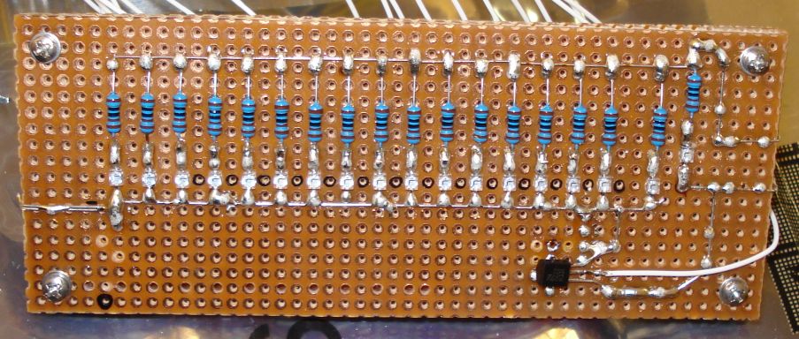
INPUT / OUTPUT
The main schematic of the input/output I have designed is shown below. Click on the picture for a bigger image.
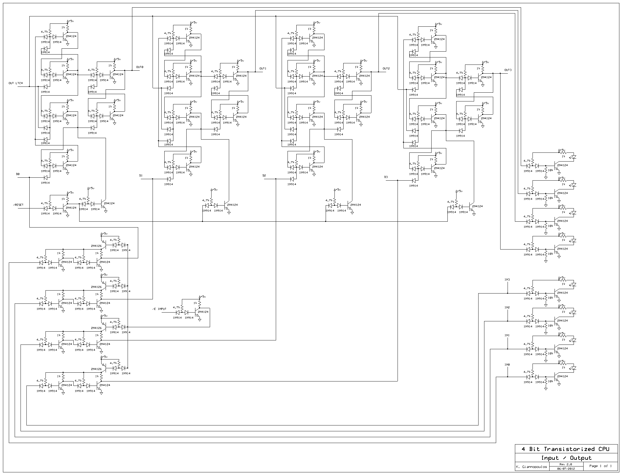
I have added monitoring of the inputs and outputs because I found this feature to be as useful as monitoring the internals of the CPU. The positive edge triggered flip-flop is shown at the top of the schematic and the I/O monitoring at the right. I have not used buffer gates on the output portion because it is not needed, as the drive capability of the flip-flop output gates is equal to that of the buffers.
For the input, buffers must be used though. The input buffers are shown at the left bottom of the schematic. The new feature introduced here, is the enable. Complement PNP transistors are used, in a configuration that allows a floating output when the gates are not enabled (output not connected to GND or VCC) and a zero or floating/one output, when the gates are enabled, depended on the input bits.
A floating output behaves like a disconnected wire. Thus, when the buffer is disabled and the flip-flop is enabled (output mode), the data inputs of the flip-flop will not be affected by any buffer inputs. Also, the outputs of the buffers will not be affected by the data bus, because both the bases and the collectors of the buffers are disconnected from the 5V. I could have used only one PNP transistor to enable all buffers but I have found that it cannot drive more than 2-3 gates in that configuration.
In the case that the buffer is enabled and the flip-flop is reset (input mode), a floating buffer output that behaves like a disconnected wire, will be seen as input-set-1 at the input diode of the next stage (input set to 5V and floating input mean the same thing, since the computer is made out of the same kind of gates). In that case, I am not really sure if a SET output will be floating or 1. Either case, the next stages will "sense" both of them as 1.
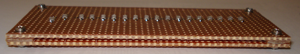
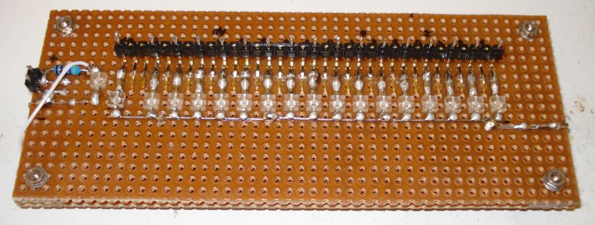
Version 2 of the input/output design has a more simplified LED display section.
Front panel
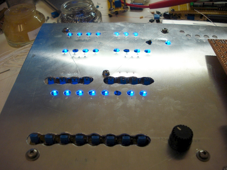
After making the programmer and the punch card reader, things have been started to get a bit messy, as there were a lot of wires coming out of the programmer. To ensure rigidity and usability, I have decided to build a front panel for the computer and tie the boards on it.

The front panel is made out of a single piece of aluminum sheet. Holes have been drilled for the display LEDs and the jumper switches and also to support the programmer board underneath. The punch card reader is mounted on the front in order to be accessible and it's cables pass through a hole to the programmer.
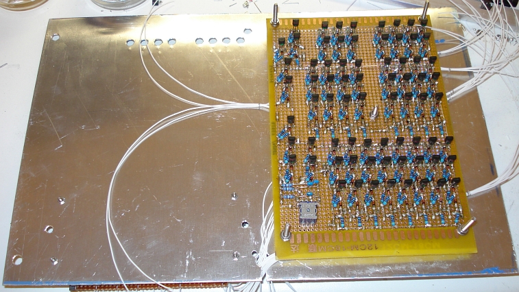
The jumper switches holes have to be made a little bit larger, to allow your finger to set up the jumpers. Some extra holes have been made as well, in order to support the I/O board LEDs later on. The lettering is done using a punch letter kit. This ensures the letters will never fade out throughout the years.