1-30MHz deluxe crystal controlled transmitter
by SV3ORA
Introduction
In this article I am going to show you step by step the construction of a high quality QRP transmitter, which I have named as NEXUS 6, in my try to explore the issues related to extremely narrow bandwidth communication. It is not just another QRP transmitter on a diet and I will explain why. The goal is to build a cost effective system that could be easily reproduced by radio amateurs, yet using simple circuit topologies that can make this system a high quality one. Extremely narrow bandwidth, phase noise, harmonic suppression and distortion are greatly considered. These parameters are not always easy to combine, as each parameter may cancel the others.
Discrete components were used where possible. Using discrete components you ensure that your construction will always be able to be serviced (as long as discrete transistors exist). Building a high quality construction is not as easy as the Medifast diet, and burning out a component that is 20 years old may not be the best thing to do especially if this component is a specific microchip that has been discontinued.
The consideration about coils is very important too. Coils and high frequency ferrite transformers are almost an essential part of any serious RF construction, as they solve many of the inter-circuit problems, but many radio amateurs do not have the right cores and the skills to build complex transformers neither the equipment to test them. In some cases, impedance mismatching is not very crucial, especially in HF bands so some transformers could be replaced with more commonly available components. In Nexus 6, I try to avoid using coils where I can. Unfortunately some coils, (like the bandpass filter or the broadband transformers) are essential and cannot be omitted.
Many radio amateurs seem to ignore factors like phase noise, distortion, harmonics suppression and bandwidth in their systems. For example, as long as a transmitter transmits they do not care about such factors too much. But if you talk about ultra low bandwidth or if you use the Nexus 6 as a backend for a microwave system, then you should consider these. Nexus 6 has been designed for QRSS operation and to test my CDW data transfer system that I have built. These systems need no more than a few hertz or tens of hertz to exchange information and they could be considered as the only fail-safe way to transfer information in ultra long distances using ultra low bandwidth. If everything else fails they will work!
Another point is that most of the QRP circuits that I have seen for shortwave is for a single band or for a few bands. In my approach I am trying to make a continuous coverage broadband system which can operate from about 1-30MHz. Making a broadband system without using complex broadband transformers is not easy and even if you succeed then you may need to carefully chose the components to ensure that the system will be as linear as possible throughout the HF bands. Broadband systems and harmonic suppression are difficult and expensive to accomplish. Sharp variable filters may be needed and this is not an easy and cheap task. The techniques used in NEXUS 6 try to reduce unwanted harmonics without compromising the broadband behavior of the circuit and without raising the budget and complexity too much.
A disclaimer notice
I have found many circuits on the web that did not work satisfactorily or they did not work for me at all. So I decided to use the working ones and perform my own adjustments to suit my needs. If you build the Nexus 6 the way I describe you, it will work. I have performed months of tests in order to build a good working system so please do not judge easily before you study or build the circuit by yourself. Everything in the schematic has been there for a reason and there is nothing that is not needed. Since I am a hobbyist in electronics though, I will be glad to discuss with you any points you think that should have been done better, so your feedback is greatly appreciated. The main source for the information to build Nexus 6 was the web. I do not have a references section in the article but I feel like I need to give credit to all these radio amateurs that have written wonderful articles to help others understand radio better. If you recognize a point from an article of yours inside this article, then you know your work has been greatly appreciated by me. Thank you!
Why QRP?
Most amateurs use approximately 100 watts of power, and in some parts of the world, can use up to 1500 watts or more. QRP enthusiasts contend that this isn't always necessary, and doing so wastes power, increases the likelihood of causing interference to nearby televisions, radios, and telephones and, for many countries' amateurs is incompatible with the regulations, which states that one must use "the minimum power necessary to carry out the desired communications." Communicating using QRP can be difficult since the QRP users must face the same challenges of radio propagation faced by amateurs using higher power levels, but with the inherent disadvantages associated with having a weaker signal on the receiving end, all other things being equal. QRP aficionados try to make up for this through more efficient antenna systems, sophisticated equipment and enhanced operating skills.
OK,
why would an amateur operator decide to operate with flea power when
most hams are using much higher power?
QRP is putting the HAM back into ham radio.
Once you get into QRP'ing, you soon learn that most QRP'ers are very
active on the air and many are also busy on the workbench building and
tinkering with equipment. There are many fun on-the-air operating
activities each month. Some are short fun contests with crazy themes,
while others may be outside "Field Day" events. Also, there are weekly
nets sponsored by several QRP clubs. QRP'ers seldom lack excuses
(opportunities) to get on the air, either for a short QSO or a fun
operating event.
Many QRP'ers build and fix their own equipment.
While you can certainly turn down the drive on an existing QRO rig and
try out low power operation, most QRP'ers find that building kits or
home brewing their own rigs is an exciting aspect of QRP. There are
many vendors and clubs that are currently producing excellent kits
designed for QRP'ers. There are probably more choices of rigs available
now than ever before. Many of these kits are very economical and are
easy to construct. Some are high performance rigs that rival and exceed
the performance of the mainstream commercial rigs.
It's fun and easy to build kits and the finished rigs are capable of
excellent on the air results. If they don't work or you have problems
later, both the vendor and the multitude of hams on the Internet are an
available resource to help get things going. Many QRP'ers become quite
confident of working on their own rigs because they gained a good
understanding of the circuit because they built the rig. Want a
challenge? Try home brewing a station accessory or a radio from
scratch. The QRP club bulletins are loaded with projects that the
average ham can build. You don't have to etch PC boards if you don't
want to. By building with either "ugly" or "Manhattan" construction
methods, rigs go together quickly and easily using basic hand tools.
QRP'ers cut the power cord.
Most of the current crop of QRP radios are very power efficient and can
be operated from a small battery. You are not tied to the power lines
when you go to the field or on a trip with your rig. A one or two watt
rig can be operated for several hours from a AA battery pack and five
watt rig will work all day (and then some) from a small gel cell
battery. It's very easy to toss a compact rig, antenna and battery into
a backpack and operate from the great outdoors. Throw a wire up into a
friendly tree and get on the air from the woods or the city park!
Likewise, a small rig fits into a suitcase easily for those trips
across the country or to distant ports of call. Ever want to be the DX
station? Pack along a QRP rig on that next trip overseas and see what
it's like to operate from the other side of the pond.
Can I really work anyone with only 5 watts or less?
Sure you can! It's actually pretty easy to make QSO's with low power.
Let's make a short comparison between QRO and QRP:
Say you have a commercial rig that has an output of 100 Watts and you
work someone who gives you a 589 report on CW. If you lower your power
to 5 watts, you will be about 2 "S Units" lower and should be 569 copy.
That's still solid copy.
The simple math for the above illustration if you're interested:
10 Watts compared to 100 Watts = 10 dB reduction
5 Watts compared to 10 Watts = 3 dB reduction
Total power reduction 10 dB + 3 dB = 13 dB
One "S Unit" = 6 dB, therefore 5 Watts is only about 2 "S units" lower
than 100 Watts.
Put that 5 watts into a gain antenna (like a beam), you will be hard
pressed to tell the difference between a 5 watt and a 100 watt station.
The FCC rules state that amateurs must use the minimum power necessary
to carry out the desired communication. Based on this rule, it may be
illegal to run 100 watts when only 5 or less is needed to make the QSO!
Why create unnecessary QRM on the band when QRP will work.
QRP is environmentally friendly!
I mentioned above that QRP rigs are power efficient. This means that
your electric meter won't be spinning as fast when you are on the air.
Also, you probably won't need to worry about RFI exposure problems.
Your little 5 watt rig isn't going to be a RF hazard to your family or
neighbors. TVI and interference to consumer electronics devices in your
home or neighborhood is unlikely. You can keep right on operating
during TV's prime time hours and no one will notice!
Improve your operating skills with QRP.
Want a thrill? Try DX'ing with QRP for an adventure. Anyone can work
Europe or Japan with one of those 100+ watt commercial rigs. Try it
with a little battery powered QRP rig that you put together yourself
for kicks! You will soon learn advanced operating techniques, like
listening, timing your calls or selecting the best transmitting
frequency. One of the many popular activities is the QRP-L Fox Hunts
where you have a two hour period to work the Fox, which is a QRP'er who
volunteers to serve as the Fox station. The Fox tries to get as many
QSO's possible during the two hours. The Hound (that's you) tries to
get through the ensuing pile-up of 100 or more QRP'ers to be heard by
the Fox. It is both fun and educational as you learn to bust pile-ups
with a five watt or less transmitter. You will quickly learn pile-up
techniques that will help earn you that rare DX QSO on the the bottom
end of 20 meters. QRP'ers also work to get every possible milliwatt
into the air by minimizing feed line losses and using efficient
antennas.
The only fail-safe communication.
I
think most of you will agree that if every other means of communication
fails, QRP will not. In the extreme cases of general power failures,
wars, earthquakes or even if someone is in the middle of the desert or
at the poles or at other distant places, you just do not have enough
power to drive your amplifiers for ever. QRP then, is the only way of
communicating with the rest of the world.
I've lost count, but there were a bunch of reasons above explaining why
QRP is pretty neat, but the main reason to try QRP is:
QRP = Little Radios, Big Fun!
Put some FUN back into your radio. Try QRP!
Why extremely narrow bandwidth and what modes of operation?
Nexus 6 has been designed to operate using as minimum bandwidth as possible, which ensures long distance communication using low powers. Using minimum bandwidth at the receiver allows you to knock out the noise, thus you can detect more weak signals, but the tuning can be quite difficult. Using minimum bandwidth at the transmitter (this is ignored by many radio amateurs) you ensure that your transmitted signal will not produce strong harmonics and also it will not interfere with others. There is a great explanation by Mark Amos about this so keep reading. You can also use the sound card of your computer in conjunction with some great DSP audio software to detect very weak signals, but in Nexus 6 I avoid using external devices as I want it to be as solid and self contained as possible.
There are quite a few modes out there that can use very low bandwidth but, as far as I know, there are only two modes that can be used to transfer information under the minimum possible bandwidth. The well known (but misunderstood by many) CW mode, which is used for text messages and the CDW mode (that is currently under development by SW3ORA) which is used for data transfer. Here I am talking about a bandwidth of a few hertz and not about 100Hz or so. Note that the minimum bandwidth that is needed to transfer information is related to different factors such as the speed of the data transfer and the keying envelope.
At this point I would like to present you a wonderful article that has been written by Mark Amos W8XR, which is one of the most complete and easy to understand explanations of CW bandwidth from my point of view. It is applied on both CW and CDW since CDW uses the same keying techniques as CW. To distinguish it from the rest of the text I have included it inside horizontal lines.
An
Intuitive Explanation of CW Bandwidth
by Mark Amos, W8XR
How much bandwidth does it take to send Morse code?
When the question of CW* bandwidth is discussed there are often
inconsistencies and inaccuracies sprinkled in among the facts. And,
while technical explanations can be found, they are typically laced
with difficult mathematics. In researching the topic, I found that
there was a lack of simple, intuitive explanations. I hope this article
serves that need.
Topics that we'll cover:
- Production of radio frequency CW
- Morse Code keying
- The keying "envelope"
- Rise and fall times
- Keying speed, baud rates
- Carrier bandwidth
- CW bandwidth
First, some basic foundation material about radio, Morse code speed,
baud rates and keying for those of you who haven’t spent much time in
this arena.
What does it take to send Morse code via radio waves?
- some kind of a radio frequency oscillator to create a carrier
frequency
- an amplifier to buffer and amplify the oscillator output
- a feedline and antenna to couple the signal from the amplifier to the
void
- a way to turn that carrier (CW*) on and off to transmit
Morse code.
We won't talk about the first three here. There are plenty of good
books and websites that explain them well - the ARRL Handbook is a
great place to start.
One obvious way to turn the carrier on and off is to use a key between
an oscillator and an antenna. Alternatively, as in some early radios,
the key might turn an oscillator on and off as we tap out our message.
Or, it might interrupt the signal from the oscillator to the amplifier.
It could also turn the amplifier on and off. It could use a combination
of these. Regardless of how it’s done, this keying is what imparts
information onto an otherwise steady (and information free) carrier.
A key is a switch - it's either on or off. If you were to tap out a
series of dits on a key hooked up to your transmitter and look at the
key's terminals with an oscilloscope you'd see something that looks
like a square or rectangular wave. If you've been around long enough,
you might even have heard one or two radios that had oscillators or
amplifiers that were directly keyed.
"Modern" radios modify the shape of this keying waveform so that it
doesn't turn on and off instantaneously. Its transitions are
rounded off so that they are less abrupt. We'll be talking a
lot about this shape. It's often referred to as the "keying envelope."
In Morse code there is a "standard word" used in speed measurement.
It's made of the letters, "PARIS." If it takes you
one minute to send PARIS, then you're sending at one word per minute.
The dits, dahs and spaces of PARIS add up to exactly 50 element lengths
long (Figure 1.) (The last seven empty elements are an
"inter-word" space.)
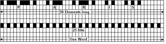
Fig. 1. "Standard" word PARIS and a simpler test word
Of course there are many possible combinations that would result in a
50 element length word - PARIS is just one that is used as a
"standard."
For the analysis below we will use an alternative and very simple 50
element length word: a string of 25 dits. Add up all the dits
and the separating spaces and you get a 50 element length word. You
could use any test word - ultimately the results would be similar - but
this simple 25 dit string might make the following discussion a little
easier to understand.
If we send our test word at the ridiculously high speed of 60 WPM
(Words Per Minute) we get one word per second.
If you had a computer before high speed internet access was the norm,
you used a modem. Modem speed is measured in terms of "baud rate".
Typical baud rates for modems started out at 110 baud in the 1970s and
increased quickly through 300, 1200, 9600, 192000 and 56000 baud in the
90's. How fast is 60 WPM in terms of baud? This requires a
look at the technical definition of "baud." It's
not critical that you understand baud rate - I'm just providing this
information for comparison purposes.
One baud is equal to one bit of information (or one "state change") per
second. There are two state changes per dit in our test word - one
where the carrier turns on, the other where it turns off.
While there are people that can copy code faster than this, there
aren't many. The record is just over 75 WPM. Our test word at 60 WPM is
about the cross-over point where other digital modes start making more
sense than the on/off keying (OOK) of Morse code.
A common conversion factor for WPM to baud is .83. So, 60 WPM * .83 is
about 50 baud. 12 WPM is about 10 baud. One of the slowest RTTY baud
rates (45.45 bauds) is close to our 60 WPM test keying rate. (In
computer signaling, the term bps has replaced baud as a transmission
speed measurement. This can get confusing because it is possible to
encode more than one bit into a state change. We'll ignore that
complication for this discussion.)
You might be thinking, "Well, if baud is state changes per second, then
wouldn't real Morse code words have different baud rates than this test
word at 60 WPM?" Yes, in fact there could be many 50 element length
words each with different baud rates because of the different number of
transitions. Morse code has variable length letters so the conversion
to baud and bits per second is a bit odd. But it doesn't really matter
to this discussion, so we'll ignore this complication too... I've only
mentioned it here to give you a frame of reference. If you
need to do a WPM to BAUD conversion, just use .83 bauds / WPM and
you'll be close.
When we send our 25 dit "test word" at 60 WPM, we will key and un-key
the carrier 25 times per second ("25 Hz", or "25 cycles per second".)
One way to think of this is that we're "amplitude modulating" our
carrier with a 25 Hz keying envelope. Just turning the carrier off and
on is a very simple type of modulation. It's also very noisy and
inefficient - it requires a lot of bandwidth. We'll talk about how much
bandwidth a little later.
However, as we know, Morse code can be a very bandwidth efficient
medium if we're careful.
Being conscientious amateurs, we would never key our transmitter with a
"square" (on/off) keying envelope. That would be seriously
"hard" keying - the kind that causes annoying "key clicks". Instead
let's try a softer kind of keying, rounding off the sharp corners of
this square, on/off keying envelope.
In fact, let's start with the "softest" possible keying. We'll use a
"raised cosine" shaped wave for our keying envelope. It will gently
increase our carrier from 0 to 100% and then back down again.
Technically, the softest possible shape is actually a Gaussian noise
curve. As shown in Figure 2., they are really the same shape with
different names.
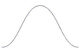
Fig. 2 Raised Cosine Waveform Fig. 3 Gaussian Waveform
So, using the very soft keying envelope from Figure 2 (or Figure 3...),
the carrier starts out with zero amplitude, slowly rises, and
accelerates as it climbs through 50%. Then its rate of climb
decelerates until it gets to 100% carrier amplitude. This
rise from 0 to 100% forms a kind of S-shaped curve (a "sinusoidal"
curve.) After reaching 100%, it begins to drop off. This
drop-off accelerates down through 50% and finally the rate of change
slows down as the end of the keying envelope is approached. The changes
to the amplitude of the carrier are smoothly changing throughout.
If we do this in 40 milliseconds, we will have sent one "dit" at 60 WPM
(we'll do the calculation for this a little later.)
This would be impossible for a human to copy. If we sent 25
of these (our test word), at 60 WPM the sound would "run together" and
the result would be an unintelligible 25 Hz hum. (Under laboratory
conditions, using a computer with digital signal processing software,
the computer might be able to "read" these 25 dits, but not you or I.)
In any case, copy-able or not, this keying envelope results in the
minimum possible bandwidth necessary to key a carrier at 60WPM.
Let's not confuse this minimum possible bandwidth with bandwidth
required for readability. What we're talking about here is the minimum
possible bandwidth that occurs when you key a carrier at 60 WPM with a
raised cosine keying envelope. (We'll talk about bandwidth required for
effective receiving some other time.)
So, how much bandwidth does it take? We need some simple mixer theory
to talk about this.
As you should remember from studying for your amateur license, when you
modulate (or mix) one signal with another, you get the sum and
difference of the two signals. Often the two original frequencies tag
along and the modulating signal is typically removed by filtering.
So, a 1 MHz carrier modulated by this soft 25 Hz keying waveform,
results in 4 resulting frequencies:
1.) 999,975 Hz (the difference: 1 MHz - 25 Hz)
2.) 1,000,025 Hz (the sum: 1 MHz + 25 Hz)
3.) 1,000,000 Hz (the carrier)
4.) 25 Hz (the modulation frequency) - this signal won't make it out of
your amplifier, much less your antenna...
So, the bandwidth this mixed signal uses is: 1,000,025 - 9,999,975 = 50
Hz. The sum and difference signals are what create the "sidebands" of
the signal. The sum results in the upper sideband and the difference
makes up the lower sideband. The carrier in the middle doesn't take up
any bandwidth (and doesn't contain any information.)
As I said, using this soft keying envelope, Morse code would be
extremely difficult for other people to copy. In order to make it more
readable, we need to "harden" the keying.
For now, let's use rise time and fall time to describe the keying
"hardness." (The "shape" of the rise and fall is important too - but
we'll keep the shape constant for now and continue to use parts of a
raised cosine shaped envelope.)
Using the softest of all possible keying envelopes, the Gausian
envelope, the rise time for a dit is 20 mS and the fall time is 20 mS.
When we send a string of 25 of these dits, this makes up what amounts
to a 40 mS wavelength. (We can check our work by taking the reciprocal
of the frequency to get the wavelength - that is we divide 1 by 25.
This comes out to .040 seconds or 40 mS; half of it is rise time and
half of it is fall time (Fig. 4.)
For this kind of soft keying, we'll call anything above 50% "on" and
anything below 50% "off".
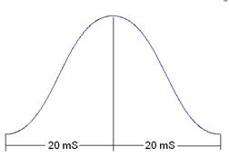
Fig. 4 One "Dit" at 60 WPM (25 Hz keying envelope.)
What if we halve the rise time and fall time to 10 mS but leave the
frequency the same?
We'll get (Figure 5.):
10 mS rise time
10 mS where the signal is at 100%
10 mS fall time
10 mS with the signal at 0.
Since the frequency is the same, 25 Hz, this whole envelope has to add
up to 40 mS. We've just sort of "stretched out" the parts of the
envelope where the carrier is 100% and where it's 0%. But we've also
narrowed the raised cosine parts for a sharper rise and fall. See
figure 5.
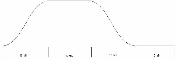
Figure 5. 10 mS rise, 10 mS at 100%, 10 mS fall and 10 mS at 0
(Still 25 Hz - 60 WPM)
During the times when the envelope is steady (at 100% and 0) the
carrier is not taking up any bandwidth: if we transmit an unchanging
1MHz carrier it won't take up any bandwidth. This is difficult for a
lot of people to accept. It seems counterintuitive ("There must be
SOMETHING there taking up bandwidth"), but it's true.
Put another way: the only time that the sidebands push out and take up
bandwidth is during a change in the amplitude of the carrier. That is,
during the time that the envelope is going up or down (where the
amplitude of the carrier is increasing or decreasing.) Ideally, when
transmitting CW, this only happens during the rise time and fall time
of the keying envelope**.
Even this smooth raised cosine envelope changes the amplitude of the
carrier, albeit slowly and gracefully - no jagged edges here. This
changing envelope causes the sidebands to push out either side of the
carrier.
OK, now let's dig just a little deeper.
The width of the sidebands (the bandwidth) has to do with the
"steepness" of the keying envelope; how fast it is changing the
carrier's amplitude. By increasing the slop of our keying waveform,
we're increasing the required bandwidth. Signaling theory folks would
argue that it's the rate of modulation - the 25 Hz modulating signal in
our example - that causes the sidebands. I've heard a number of
arguments about this assertion.
You're welcome to look at it this way, but consider this: what is
really changing when the modulation rate changes? It's the steepness of
the rise time and fall time of the keying envelope. Here's an example.
What if we double our initial keying rate from 60 WPM to120 WPM (that
is, increase our modulating frequency from 25 Hz to 50 Hz)? What would
the leading and trailing edges look like?
This is easier to see than it is to talk about. Take a look at a 25 Hz
cosine shaped wave overlaying a 50 Hz cosine shaped wave in Figure 6.
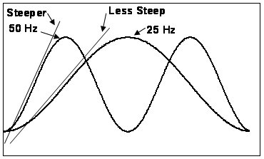
Fig. 6 It's the "Steepness" that counts.
Notice anything interesting about how steep the 50 Hz wave is as it
goes from 0 to peak?
You might say the rate of change is "twice as steep" as in the 25 Hz
wave - and you'd be right. In order to fit 50 cycles into the same
second that our 25 Hz signal fits in, each 50 Hz wave has to have
"steeper" sides than the 25 Hz waves - in fact, twice as steep.
Again, it's the rate of change of the carrier due to the
keying envelope that counts. The slope, or the rate of change, is a
measure of the "steepness" of the rise or fall time. For a modulating
(or keying) waveform, twice as steep means twice the bandwidth.
Some might still argue that the increase in the modulation rate is
causing this.
Of course there's a kernel of truth there. If you increase the rate of
modulation, you increase the steepness of the modulating wave form (as
is evident in Figure 6.) But, it's actually the steepness of
the rising and falling envelope that causes the sidebands (and
consequent bandwidth) not the signaling rate. If you had only one wave
at this frequency, the bandwidth required would be exactly the same as
the continuous train of waves in our example.
Technically, it's not just the steepness of the rise time and fall
time. More precisely, it's the rate of change of any part of the
envelope. For instance, if instead of a nice smooth rise from 0 there's
an abrupt change, this abrupt change will increase the bandwidth. A
saw-tooth, triangular or stepwise envelope would cause a much higher
bandwidth signal than our raised cosine envelope. If the carrier is
modulated in some other way the bandwidth could also increase (for
instance if the signal has some "chirp") but in this analysis we're
only considering bandwidth due to the keying envelope.
You need to get to the point where you can say, with conviction: "It's
the shape of the keying envelope that causes a keyed CW signal to take
up bandwidth. An un-keyed/un-modulated CW signal takes up no bandwidth."
How can we determine how wide our signal will be based on the rise and
fall times of the keying envelope? This section talks about a way to
estimate this.
When we harden the keying by increasing the slope of the rising or
falling part of the keying envelope, we're pushing out the sidebands as
if we were modulating our carrier with a wave that has the same slope
and shape as the rising and falling parts of the modulation envelope.
This is a little tricky, but an example should help.
In the first scenario above, we halved the rise and fall time to 10 mS
apiece but kept the keying rate the same. By cutting the rise and fall
time in half, it's as if we're now modulating our carrier with a 50 Hz
sine wave (even though the rise time and fall time are separated by
periods of no change.) The sidebands push out to +- 50 Hz, requiring
100 Hz of total bandwidth to send this same 60 WPM word.
Another way to say this: if we keep the rise time and fall time of our
envelope and take out any parts where the envelope is not changing
(when it's at 100% and 0% for instance), we can figure out this
waveform's frequency (based on its wavelength) and use that to estimate
required bandwidth. So, for instance, a 50 Hz sine wave has a rise time
and fall time of 10 mS each (1 / 50 is 20 mS.) If our
envelope has the same rise time and fall time as a 50 Hz sine wave, and
it's rise and fall have the same shape as the rise and fall of a 50 Hz
sine wave, then we can treat it like a 50 Hz signal to compute
bandwidth.
Remember: when the keying envelope isn't changing, there are no
sidebands and no bandwidth - sidebands and bandwidth only occur during
the times when the keying envelope is changing.
If we halve the rise and fall times again (to 5 mS), it's as if we're
modulating our carrier with a 100 Hz waveform (5 mS rise time + 5 mS
fall time = 10 mS; 1/10 mS = 100 Hz). The sidebands go out to +- 100 Hz
for a total of 200 Hz bandwidth.
Of course in the real world, not many radios use smooth Gaussian
keying, as we do here. Typically they use a resistor-capacitor "filter"
used to soften up the rise and fall. Why is this still done? The
engineering isn't that hard anymore - it's a matter of economics: it
would cost more per radio for manufacturers to add a Gaussian keying
envelope.
An RC filter has sharper edges and consequently causes more bandwidth
to be used. It's obviously better than just using a square
keying envelope. However it's still pretty wide and if the rise time
and fall times are less than 5mS or so, it will be pretty "clicky" even
on some high-end radios.
Ok, so how much bandwidth would a "square" keying wave take?
Way too much. The rise and fall times of a square wave are "infinitely"
steep. This kind of keying results in a very wide signal with lots of
noise with every key down and key up.
It's as if you're modulating your carrier with a very high frequency
signal - sidebands are pushed out to infinite bandwidth. Well, maybe
not infinite, but a lot more than the other amateurs up and down the
band deserve. If you're doing this on 40 meters, some of your key
clicks could be making it up to the 20 meter band -- or maybe even your
phone or your neighbor's TV, depending on how much power you're trying
to pump out.
Not only is this inefficient - there is wasted power in those
"infinite" sidebands - in most parts of the civilized world it's
illegal. The exact bandwidth is tricky to calculate, because of things
like the bandwidth of your transmitter, filters that might be in the
signal path, your amplifier linearity, the width of the pass-band of
your tuner, the bandwidth of your antenna, etc.
Regardless, it's wide enough to get you in trouble. So pay attention to
your keying envelope. Don't key that homebrew rig with a square
envelope or any envelope that has a rise time or fall time less than 5
mS or so. Also, if possible the rise and fall should be shaped like our
raised cosine curve. If they're exponential curves (like you get with
an RC filter) you will be taking up more bandwidth than is absolutely
necessary.
Here are a couple of key takeaways:
- If you take nothing else from this article, you should be able to say
with confidence "The bandwidth of a typical CW signal depends on the
shape of the keying envelope."
- The hardness of the keying is greatly influenced by the rise and fall
time of the keying envelope. A rise and fall time of 5mS or more will
result in a readable signal at reasonable bandwidth.
- Sidebands of a CW signal are caused by keying (an unmodulated carrier
requires no bandwidth.)
- You can estimate the bandwidth required by analyzing the shape of the
keying envelope ("removing" the parts that are unchanging and
calculating the frequency of the remaining portions.) This applies with
"soft" keying. Using "harder" keying increases the required bandwidth
dramatically.
- Lots of people like to argue about these points even if they don't
really understand them. It's best to just "walk away" from these
arguments, unless you just like to argue. Little exchange of knowledge
is likely to occur, even if it is somewhat entertaining...
*Technically, CW means "Continuous Wave." When radio amateurs talk
about CW they're really talking about on/off keying (OOK) of a
continuous wave. Certainly there's nothing "continuous" about a keyed
carrier; it stops and starts all the time. As mentioned above
technically, CW doesn't take ANY bandwidth at all if it's not being
modulated. In this article, we use the term CW in the amateur sense.
**Of course in the real world there are complications, like phase
noise, jitter, FM, etc. but that's another story and doesn't really add
to this discussion in any meaningful way.
A few notes by SW3ORA on the article:
To
overcome the confusion by many readers, I would like to say (correct me
on this) when the writer talks about "an unmodulated carrier requires
no bandwidth", he means that an unmodulated carrier does not have
on/off transitions but it is either switched on continuously or it is
off (transmitter continuously off, i.e. no carrier). No transitions,
meaning no bandwidth is required to transfer anything, as no
information is transmitted.
This does not mean that an unmodulated transmitter that is continuously
switched on, will not take up bandwidth on the specific frequency of
the radio spectrum. Every signal in the radio spectrum consumes some
bandwidth, even if it is unmodulated. The bandwidth of an unmodulated
carrier is less than that of a modulated one and it is defined by
different factors, one of them being the phase noise of the transmitted
signal.
From the technical point of view, to very slowly change between off/on
state in the CW/CDW data sequence and hence to decrease the bandwidth,
you can have a circuit that slowly varies the output power of your
transmitter. For example, if you press your key down, then this circuit
will start increasing your transmitter's power from zero, up to the
full power. When you release the key, the circuit will decrease the
transmitter's power from full power to zero. How fast this change will
occur can be decided by the operator, considering bandwidth and data
speed. This is one of the ways in which you can achieve minimum
bandwidth required to transmit CW/CDW information. Of course the data
rate is very slow if this increasing/decreasing of power happens
slowly, but then, minimum bandwidth is used.
The Nexus 6 transmitter
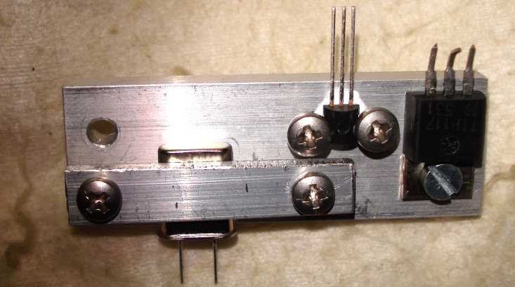
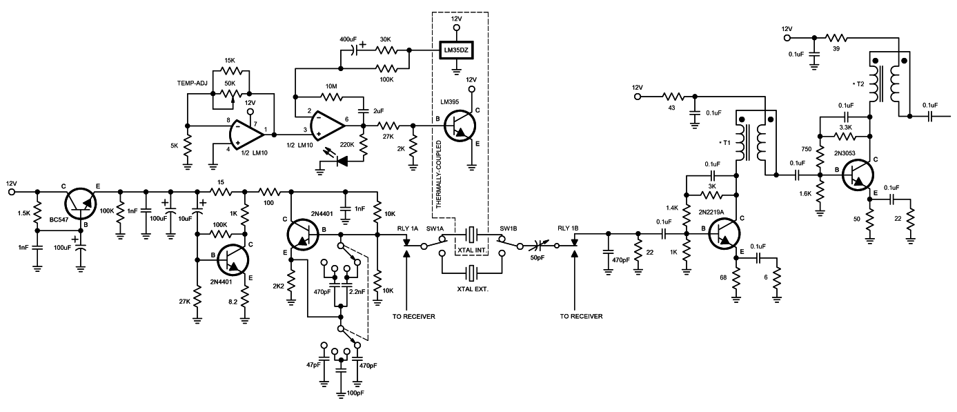
After this long helpful preface I think you must be able to understand now the issues around the Nexus 6 QRP transmitter, so let's get now on to the real stuff. Nexus 6 is currently under development so I will present you the transmitter step by step as I develop it. Let's start with the transmitter. The picture below shows the crystal oscillator and the oscillator PSU of the Nexus 6.
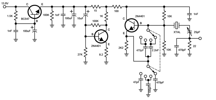
Crystal oscillator and oscillator PSU of the Nexus 6
The picture shows an ultra low phase noise low distortion crystal oscillator, along with it's power supply. This type oscillator has been discussed in detail with Charles Wenzel from Wenzel Associates, to define it's performance. You could expect a phase noise better than -150dBc from this circuit and this is far better than any PLL can do. That is why I use a crystal oscillator and not any other kind of PLL/DDS. The trick is not to overload the crystal and thus degrade it's high-Q. The crystal used in that place, acts as a filter too, which helps eliminating some of the unwanted signals at the output of the oscillator.
The 25pF variable capacitor is used to shift the frequency of the crystal a few tens or hundreds of Hz in order to achieve fine tuning. Do not shift the crystal frequency too much or the phase noise will be degraded. I have performed different power and frequency measurements on the oscillator to understand it's linearity, but since linearity may be depend on the specific crystal used, I would not like to present the measurement results here. In general, the oscillator is more linear at 7-18MHz and presents higher output levels, whereas the power level is a bit reduced at the low and high ends of the shortwave bands (160m and 10m).
As far as concern the mechanical construction, use a two-pole four-position panel switch to switch between different bands. Use a panel mount crystal holder in order to change crystals for different bands. Try to keep the leads lengths as short as possible. The crystal and the variable capacitor will be switched between the oscillator and the receiver filter using relays, but I will show this later on. For the time being, leave some empty space for a relay there. Use a panel mount air variable capacitor, preferably silver plated, in order not to degrade the Q of the crystal too much. If you cannot find silver plated capacitors use aluminum or nickel plated, but always use air dielectric ones. Warning, both poles of the variable capacitor must be insulated from the chassis. Additionally, connect the capacitor such as the pole that you touch with your finger is connected at the 22 Ohm resistor side and not at the oscillator side! If you do it the other way, the oscillator frequency will change a bit every time you touch the capacitor with your finger. Even if you use an insulating knob for the capacitor, it is a good idea to connect it as I mentioned.
The power supply of the oscillator is composed of a BC547 transistor and a 2N4401. The BC547 section behaves like a capacitor multiplier, multiplying the 100uF at the base of the transistor with the 100uF shunt capacitor, to give a total of 10000uF. This should suppress any potential hum, but to achieve a lower phase noise oscillator I have added the 2N4401 section taken out from Wenzel Associates.
System
designers often find themselves battling power supply hum, noise,
transients, and various perturbations wreaking havoc with low noise
amplifiers, oscillators, and other sensitive devices. Many voltage
regulators have excessive levels of output noise including voltage
spikes from switching circuits and high flicker noise levels from
unfiltered references. The traditional approach to reducing such noise
products to acceptable levels could be called the "brute force"
approach - a large-value inductor combined with a capacitor or a
clean-up regulator inserted between the noisy regulator and load. In
either case, the clean-up circuit is handling the entire load current
in order to "get at" the noise. The approach of the 2N4401 circuit
described here uses a bit of finesse to remove the undesired noise
without directly handling the supply's high current.
The key to understanding the "finesse" approach is to realize that the
noise voltage is many orders of magnitude below the regulated voltage,
even when integrated over a fairly wide bandwidth. For example, a 10
volt regulator might exhibit 10 uV of noise in a 10 kHz bandwidth - six
orders of magnitude below 10 volts. Naturally, the noise current that
flows in a resistive load due to this noise voltage is also six orders
of magnitude below the DC. By adding a tiny resistor, R, in series with
the output of the regulator and assuming that a circuit somehow manages
to reduce the noise voltage at the load to zero, the noise current from
the regulator may be calculated as Vn/R. If the resistor is 1 ohm then,
in this example, the noise current will be 10uV/1ohm = 10uA - a very
tiny current! If a current-sink can be designed to sink this amount of
AC noise current to ground at the load, no noise current will flow in
the load. By amplifying the noise with an inverting transconductance
amplifier with the right amount of gain, the required current sink may
be realized. The required transconductance is simply -1/R where R is
the tiny series resistor.
The 2N4401 circuit is suitable for cleaning up the supply to a low
current device. A 15 ohm resistor is inserted in series with the
regulator's output giving a 150 millivolt drop when the load draws 10
mA - typical for a low-noise preamplifier or oscillator circuit. The
single transistor amplifier has an emitter resistor which combines with
the emitter diode's resistance to give a value near 15 ohms. The
regulator's noise voltage appears across this resistor so the noise
current is shunted to ground through the transistor's collector. The
noise reduction can be over 20dB without trimming the resistor values
and the intrinsic noise of the 2N4401 is only about 1 nanovolt per
root-hertz. Trimming the emitter resistor can achieve noise reduction
greater than 40 dB.
Stabilizing the oscillator
Now that we have a low noise crystal oscillator we must try to achieve greater frequency stability. When dealing with ultra low bandwidth, our oscillator must be very stable, in order to minimize frequency drift and the need for automatic signal following filters. A good PLL or DDS will be of much use here but quite noisy, so the crystal solution has been chosen. Remember we use standard two-pins crystals and not the four-pins crystal modules that produce TTL signal. The greater parameter that affects crystal stability is the change in ambient temperature. To keep the ambient temperature stable we must use a device called crystal oven. A proportional temperature controller, commonly known as crystal oven, can be made with an LM34 and a few additional parts. A suitable crystal oven is shown in the picture below.
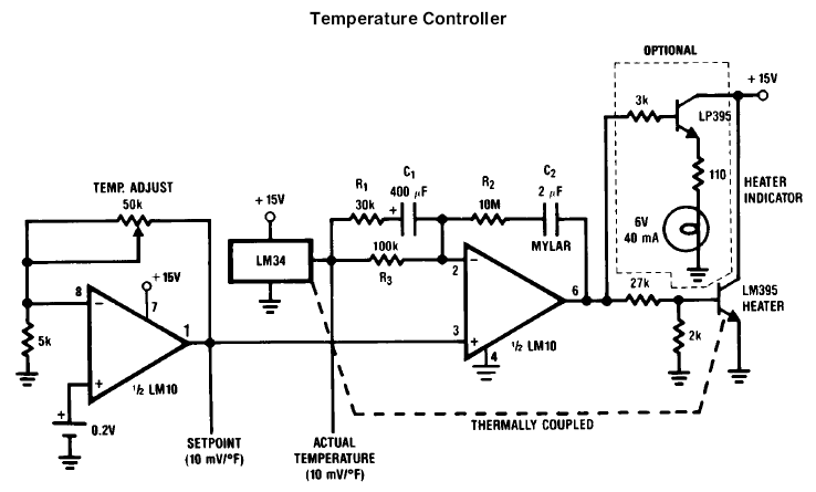
Here, an LM10 serves as both a temperature setting device and as a driver for the heating unit (an LM395 power transistor). The optional lamp, driven by an LP395 Transistor, is for indicating whether or not power is being applied to the heater. When a change in temperature is desired, the user merely adjusts a reference setting pot and the circuit will smoothly make the temperature transition with a minimum of overshoot or ringing. The circuit is calibrated by adjusting R2, R3 and C2 for minimum overshoot. Capacitor C2 eliminates DC offset errors. Then R1 and C1 are added to improve loop stability about the set point. For optimum performance, the temperature sensor and the crystal, should be located as close as possible to the heater to minimize the time lag between the heater application and sensing. Long term stability and repeatability are better than 0.5F.
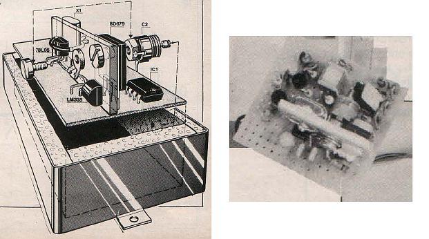
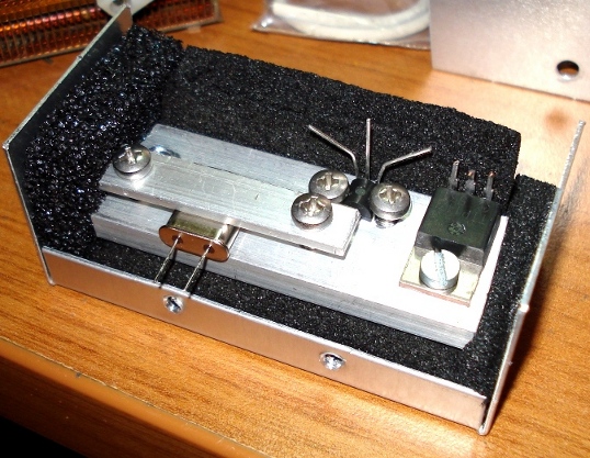
The mechanical construction of the crystal oven is not difficult. Make a small box and insulate it with some kind of thermal insulator. Any material that can thermally insulate the box (eg. foam) will do. Search your local stores for something suitable. Then get a thick piece of aluminum (about 2cm x 4cm x 5mm or more) and mount the sensor, heater transistor and crystal on it, as close as possible. The final construction should look something like the picture below, that has been taken from another crystal oven project.
In my construction, I chose to put only the crystal, the heater transistor and the sensor inside the oven and the rest of the circuit, outside. I do not really like to overheat the operational amplifier and the rest of the components and also this allows for easier changing of crystals, as I used hand-wiring and no PCB. Since Nexus 6 is a broadband system, we have to be able to change crystals often. I faced this problem when making the crystal oven, as it is difficult to change crystals that are mounted inside an enclosed insulated box. To overcome this, I made a special construction that allowed me to change the crystal by just unscrewing a screw, accessible from outside the oven box. The illustration of this technique is shown below.
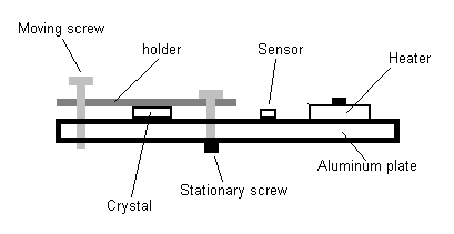
The picture shows the aluminum plate as seen from one narrow side. You can see how the different components are mounted on it. To hold the crystal stable, another piece of thinner aluminum sheet is used, mounted with two screws onto the aluminum plate. The aluminum sheet (holder) should be made such that it can move freely when there is no crystal. One of the screws is the stationary, holding the holder just above the crystal, loosely. By screwing the moving screw you can make the holder to hold the crystal tight on the plate. A quick note, do not press the crystal too hard on the plate as it might brake it's case. Just a low pressure will be fine, enough for keeping the crystal firm on the plate. When making the box for the oven, leave a small hole on it, so that the crystal can slide trough it and changed easily. This hole serves also as connection to the crystal pins. Then make another hole to be able to access the moving screw with a small screwdriver. Note, the two holes made on the box are small and no significant heat loss occurs. The next pictures show how this was made:
Assembly of the crystal oven elements
Overal assembly of the crystal oven in the box (semi-finished)
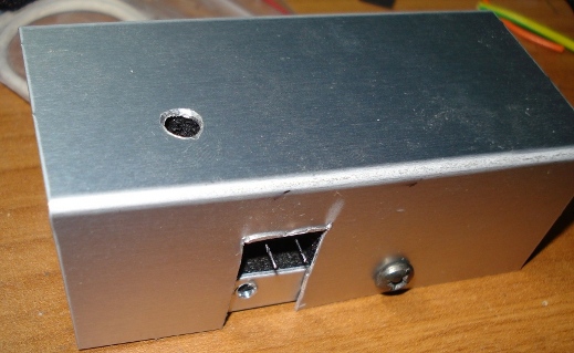
Finished crystal oven enclosed in the box
The process of changing the crystal is quite simple:
Unsolder the crystal from the circuit (if using a crystal holder base, you do not need to do so).
Unscrew a bit the moving screw.
Slide the crystal out of the box.
Slide another crystal back in.
Screw the moving screw.
Solder the new crystal in the circuit (if needed).
It is not as easy as changing crystals without using an oven but this is much easier than changing the crystal inside an enclosed oven box. This is the price to pay for the extra stability though. In Nexus 6 there are two options. You can either chose between an external crystal that does not use crystal oven, or you may use the internal oven crystal. Sometimes when we do not need to use ultra low bandwidth, an ultra stable oscillator may not be needed, so it is nice to be able to change bands very easily and that is why the external crystal option is nice. Note, since you have to keep the crystal leads as short as possible, you have to mount the crystal oven as close as possible to the rest of the oscillator circuit and capacitor selector rotary switch. Thus, try to make the oven box as small as possible.
Now that you have a very clean and stable broadband oscillator, it is time to think about amplification of it's low output signal level (~0.2Vpp-0.4Vpp). A multi-stage transistor amplifier can be used to raise the output to a level that will be able to drive a power amplifier (>10mW). Class-A amplification is used where possible through the chain of the transmitter stages (buffers and power amplifiers) although it is known that CW (and therefore CDW) does not require class-A amplifiers. Also, this leads to a very inefficient use of power, but for QRP operation it can be acceptable. I chosen to use class-A amplification where possible because of it's advantages which are the low distortion of the amplified signal, high linearity, lowered harmonics produced and high tolerance in reflected power due to impedance mismatch. Well designed class-A amplifiers may not need output low pass filters, although it may be a good idea to use output filtering. The operation of the final amplifier is an issue though. Since it consumes most of the power and weight of the system (because of the heat sink, especially in class-A) and it is quite costly, great care has to be given in the choice of whether to choose class-A amplification for the final stage or not.
At this point I would like to present a few considerations about amplifiers. I have found a wonderful simple to understand article from Amplifier Research that discusses the issues behind broadband amplification. I have included it inside horizontal lines to distinguish it from the rest of the article, as before.
The quest for the ideal rf amplifier.
The basic function of a power amplifier is always the same: to boost a low-power signal to a higher power level, to be delivered to the amplifier load. Because that role is so fundamental, it's tempting to view amplifiers as simple black-box devices, with an input, an output, and a constant amplification factor. In many instances, the black-box approach provides an adequate picture.
It fails, however, when the demands placed on an amplifier are extreme. Hardest to satisfy is the requirement for maximum capability of two or more conflicting parameters, such as the demand for broad bandwidth and high power in the same package.
Bandwidth versus power
The demand for broadband, high-power capability has spawned a bewildering variety of amplifiers. Part of the problem is in the bandwidth limitations of power devices themselves. In any device, gain falls off at higher frequencies, largely as a function of internal parasitic capacitance. Eventually a frequency is reached where gain falls below unity, and the device stops functioning as an amplifier. To extend the bandwidth, the designer must sacrifice the size--and, with it, the power-handling capability.
Considerable effort has gone into development of output devices capable of high-frequency operation and power handling, but the conflict between these parameters has never been fully resolved. The amplifier designer faces a clear limit in the gain-bandwidth product and power capabilities of the devices, and the necessity for tradeoff and compromise in the circuit.
Along with device limitations, the designer must contend with another aspect of the broadband/high-power dilemma--the tendency for high-gain, untuned amplifiers to break into oscillation. This is of considerable importance in broadband amplifiers, where design calls for stable operation over a bandwidth often of several decades. Combined with this is the frequent requirement that the amplifier be stable under conditions of severe mismatch in the load.
Designing for broad bandwidth and stable operation within device limitations is the designer's real job--and headache. But it is exactly in this area where the designer makes a major difference in amplifier performance. Here is an opportunity to create a circuit that gets the maximum out of available devices, perhaps advancing the state of the art.
Understanding amplifier specifications
With a basic understanding of the parameters that have to be traded off in designing an amplifier, and an understanding of what the specifications mean and how they are stated, the user can select an amplifier with confidence that it will do the job it's intended for.
How broadband amplifiers are rated.
The power rating
High-power rf amplifiers are usually rated for cw (continuous-wave) operation. Pulse power (see box later in this section) is not an accurate indication of an amplifier's capability, simply because of the variables involved. Rating for cw operation gives the user an understandable figure on which to base his judgment--if, that is, the methods of rating are known.
A simple statement of the power output of an amplifier, expressed in watts or dBm, is not enough to describe the amplifier's capability. Output power varies with frequency in any amplifier. The degree to which it varies allows a certain flexibility in specifying output. For this reason, the user should know how the given figure was chosen, and the tolerances within which it fits.
Stated power can represent maximum power at a specific frequency, nominal power over the amplifier bandwidth, or minimum power available at any frequency within the bandwidth. The graph illustrates the differences that can exist in power claims for a given amplifier.
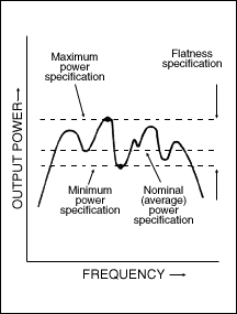
Clearly, the way the designer rates his amplifier makes a difference. This depends to some extent on the intended use; certain ratings make more sense than others in particular applications. A minimum power rating guarantees availability of at least the full rated output over the entire bandwidth. This is the most desirable rating for the bulk of high-power rf applications, because it allows for headroom above a consistently predictable figure. Excess power capability is rarely a complaint.
In some special cases, it's more meaningful to specify nominal power. Frequency tuning of apparatus, for example, calls for "ballpark" power from the amplifier. In this application, the ballpark is the flatness specification, and the quality of the flatness specification is as important as, or more important than, the absolute power being delivered to the load. Knowing the nominal power rating and the flatness specification, the user can still safely assume a minimum figure for output. Amplifiers rated in this way will always deliver power greater than the rated power minus the total flatness specification.
While it's possible to calculate minimum power if both a maximum power rating and a flatness specification are given, maximum ratings tend to be deceptive figures. They sound good; they also carry the implicit admission that, over most of the bandwidth, the actual output will be less than rated output. If no flatness specification is given, minimum performance remains entirely undefined.
Amplifier Research rates most of its amplifiers by minimum power, so the user can always predict minimum performance. Ratings are also given with a flatness specification, usually �1.5 dB; conservative ratings overall give the user an extra margin of flexibility.
One more consideration regarding output power: the drive level required to obtain rated output. This can vary widely; in the worst case, the user can find himself unable to get full use from an amplifier simply because he can't provide enough signal. All AR amplifiers are designed to require a maximum of 1 mW input for full rated output. They will withstand twenty times rated input without damage.
The amplifier bandwidth
The upper and lower frequency limits of an amplifier are defined--in Amplifier Research specifications--as the frequencies where the rated output falls below the value of the minimum power specification, or below the range of the flatness specification.
Amplifier manufacturers don't always spell out the methods they use to determine bandwidth; some amplifiers, for instance, may be rated at the "3 dB down" points. These are the upper and lower frequencies at which output falls below the rated power by more than 3 dB. Because this figure is not clearly definitive, the prospective buyer should know how the designer has arrived at his specification.
"Instant" bandwidth
One consideration which is not generally given as a part of the bandwidth specification, but which is critically important to the prospective buyer, is a factor described as "bandwidth availability." In the wide variety of rf power amplifiers on the market, there are models that have a serious limitation in certain applications--they require bandswitching or tuning at the frequency being worked, or under varying load conditions.
Such amplifiers aren't necessarily useless; they are unsatisfactory in applications calling for frequency-swept output (rf susceptibility, instrument calibration) or applications requiring constant changes in load or frequency (filter tuning, antenna trimming). In these applications, the continual need to re-tune becomes tedious and time-consuming, and may add a factor of uncertainty to the procedure.
Good designing here can provide instantly available output at any frequency in the operating spectrum--"instant" bandwidth. The stability and sweep capability implied by instant bandwidth are important factors for the prospective buyer to understand. An amplifier's stability assures the predictability necessary in research, testing, and calibration applications. Sweep capability--even if the application doesn't absolutely require it--means entirely stable, instantly available output power anywhere in the operating spectrum that the procedure calls for.
Amplifier linearity
Linearity is the ability of an amplifier to deliver output power in exact proportion (the gain factor) to the input power. Linear amplifiers are required in AM applications, for example, where the linearity specification indicates how hard the amplifier can be driven before distortion appears in the output.
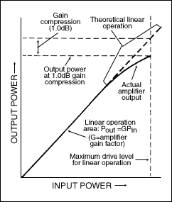
Gain compression
Non-linear response appears in an amplifier when the outputs are driven to a point near saturation. As this level is approached, the amplifier gain falls off, or compresses. The tracking relationship between output and input levels is a direct function of the gain factor; when the gain compresses, the amplifier's linearity is lost.
The linearity specification can be expressed as the output level at which the gain compresses by a given amount. Amplifier Research specifies linearity at the 1.0 dB gain-compression point, illustrated in the input vs output graph shown here.
Occasionally, an amplifier will be rated for both linear and non-linear operation. Non-linear amplifiers--for instance, those used in pulse mode or FM operation--are often driven at saturation to achieve the desired flatness specification. In amplifiers rated both ways, the linear output will always be some figure well below the saturated, non-linear output. If an amplifier is designed solely for non-linear use, however, the prospective buyer should know that it may not be at all suitable for linear applications. Operation of the output stages at a level below saturation will, in some cases, seriously affect flatness.
Harmonic distortion
All amplifiers create harmonic distortion (multiples of the fundamental frequency) to some degree. It shows up as a power loss in the fundamental, and is caused largely by non-linearity in individual stages. While it isn't entirely avoidable, the extent to which it occurs is still a matter of design, and therefore still in the hands of the designer. A number of techniques can be used to minimize harmonic distortion; AR has developed technology that incorporates these methods--often in combination--into high-power, broadband design.
Class A operation of small-signal stages, and--where possible--output stages, produces the lowest distortion figures. For higher-power solid-state applications where class A operation isn't feasible, class AB push-pull outputs are employed conservatively to achieve nearly comparable distortion levels. Harmonic filtering, particularly in amplifiers operating over a narrower bandwidth (less than one octave), is effective in reducing harmonic components in the output. Finally, the designer--with careful design and layout of the circuit--can shape gain and frequency in the amplifier to introduce the least amount of distortion.
Harmonic distortion is specified as the harmonic content of the overall output. The actual specification is usually a statement--in dB--of how far below the fundamental the harmonic content lies at rated output.
Intermodulation distortion
Intermodulation distortion is, like harmonic distortion, always present to some degree in any amplifier; again, the culprit is non-linearity. A device operating with any degree of non-linearity and passing two or more signals acts as a mixer and introduces sum-and-difference products of the applied frequencies. Many of the same techniques described above are used to minimize intermodulation distortion, although IMD is generally not as important a consideration in broadband rf power applications as is harmonic distortion.
The expression of intermodulation distortion is somewhat more difficult than that of harmonic distortion; the variables involved--the number of tones and their relative power, frequency, and separation--preclude a simple procedure for providing a meaningful figure. To overcome this difficulty, Amplifier Research uses the intercept-point method, and the amplifiers which have an IMD rating give it at the third-order intercept point.
Amplifier protection
When the designer considers the ability of his circuit to withstand reflected power from a load mismatch, he makes a decision--one which drastically affects an amplifier's usefulness in many applications.
An easy way of protecting the circuit from a high VSWR is to design it to shut off under adverse conditions. This works; but it also has the effect of taking a large degree of freedom out of the hands of the user. In applications where adverse conditions are the norm--testing and aligning power filters, for instance--the load is rarely matched to the amplifier. If the amplifier shuts down immediately under adverse load conditions, the user is left with the tedious process of trial-and-error to bring the load close enough to the correct impedance to allow amplifier operation.
By combining good design techniques with conservatively rated devices, however, the designer can come up with a circuit that will continue to operate under worst-case conditions. This is more than a nicety; ability to withstand high VSWR loads means that the amplifier output stages can completely absorb reflected power, and still function. The amplifier therefore cannot be damaged by poor cable connections, faulty cables, or any of the myriad other conditions that can be expected in normal use. And because the amplifier will work into any load condition, the user has full operating capability for any conceivable application.1
Reading between the lines
Given the availability of high-quality, state-of-the-art devices, the major differences in the amplifiers on today's market boil down to a matter of design excellence. Clearly stated, conservative power and bandwidth ratings imply conservative design techniques--and the availability of headroom in the design itself. Instant bandwidth and imperviousness to high VSWR loading indicate a level of design excellence that assures the user maximum reliability and flexibility.
1For further reading see Application Note #27
Amplifier
Research
U.S. and Canada: call toll-free direct to applications engineering:
1-800-933-8181 � 160 School House Road, Souderton, PA 18964-9990 USA �
TEL 215-723-8181 � FAX 215-723-5688
For engineering assistance, sales, and service throughout Europe, call
EMV: Munich, 89-614-1710; London, 01908-566556; Paris 1-64-61-63-29.
� 1996 Amplifier Research
Now you know why Class-A amplification is best, provided that you can afford cost, weight and power consumption. But consider the cases that I have described earlier, where class-A amplification may not suit your needs. Also, do not be confused, a linear amplifier can be class-A as well as class-AB one and it can be single ended or push-pull in topology. A 300W broadband amplifier kit that I own, using two power transistors in push-pull configuration operates in class AB (actually it would be not feasible to have a 300W pure class-A amplifier).
For the amplifiers, I tried to find suitable circuits without transformers. Almost every transformer-less solution seemed to work for a few bands but not for the whole HF bands. I also could not manage to achieve an output power of 50mW out of the buffers that I tried. Maybe I tried to drive these amplifiers with very low signal levels or maybe these were not intended for such output powers. It seems that these so called "broadband transformers" solve many of the problems related to bandwidth, linearity, matching etc. A final amplifier with a more sophisticated output transformer may be capable of delivering as much as double the output power! So I have decided finally to use these transformers. Believe me, they worth the extra pain for such a work they do. But do not be scared about them, instead of many articles I have found over the internet, that do not describe the process of making such a transformer, I am going to explain the process of making the transformers used in detail, so you can wind yours easily. Also, I have chosen to use relatively easy to wind transformers using small ferrite cores. The next schematic shows the transmitter up to the second buffer amplifier.
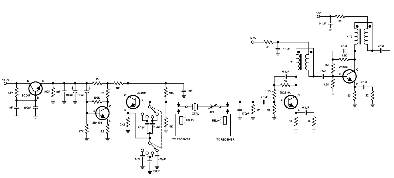
Transmitter section up to the second buffer amplifier
Notice the addition of the relay to switch the variable capacitor and the crystal to the receiver section. Also, the variable capacitor has been changed to 50pF to allow for a greater frequency shift, but as I mentioned earlier, do not shift the crystal frequency too much. The first buffer amplifier uses a 2N2219A biased in class-A operation to boost the signal of the oscillator to about +5dBm. Like every buffer amplifier, this amplifier also helps to stabilize the oscillator, by buffering it's signal before driving the next buffer or the power amplifier. The theoretical gain is about 21dB from 500KHz to 50MHz (modeled up to 3dB attenuation limit). DC biasing puts about 20mA through the 2N2219A. If you want to experiment furthermore you can adjust the 1.4K and 3K resistors for desired gain, standing current and input impedance. With the values given, output impedance is about 50 Ohm.
The second buffer amplifier uses a 2N3053 biased in class-A operation to theoretically boost the signal of the first buffer amplifier to about +20dBm. The gain of the amplifier is about 15dB and the input and output impedances about 50 Ohms. DC biasing puts about 39mA through the 2N3053. Distortion starts with input above 0.8Vp and the power output with 0.6Vp drive is about 106mW undistorted. Note, the actual total output power in the chain up to this point will be variable throughout the HF bands. This reduced and variable output power is mainly due to the low oscillator output level and it's variance in different bands. It is enough to drive most power amplifiers though and if using a high gain one, reduction of power may be needed before driving this power amplifier. Also for extremely narrow bandwidth operation the transmitter output power may be chosen to vary from zero up to full power as described before. The control of the output power of the second buffer amplifier may be a good point for controlling the output power of the transmitter, so great linearity throughout the HF bands may not be of much importance at this point.
T1 and T2 are exactly the same. They are 8 bifilar turns on a small ferrite toroid such as T37-43 or T50-43. I have found the wire diameter and toroid not to be too critical. Almost most of these small 1cm toroids you may find in your junk box will do, with similar results. The only thing to take care is to use ferrite toroids and not iron powder ones, as the last ones have more loses and they may be not so suitable for RF. I have tested two transformers, the one with T37-43 and 8 bifilar turns of 0.3mm wire diameter and the other with T50-43 and 8 bifilar turns of 0.8mm wire diameter. Both worked for 1-30MHz range, but the T37-43 proved to be better in terms of output power and linearity through the HF bands, so I recommend these! The procedure of constructing them is very easy like shown in the first picture below (note the first toroids shown, are from another project and are shown as a demonstration only). The second picture shows the actual winded transformer (T50-43 option) for the buffer amplifiers, semi-finished.
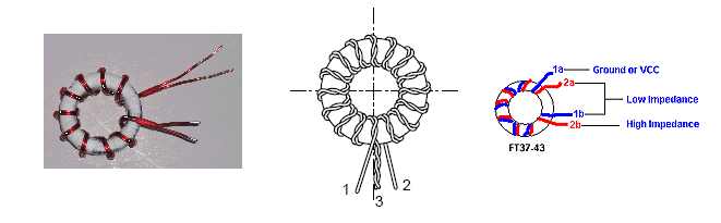
An example of broadband transformers construction
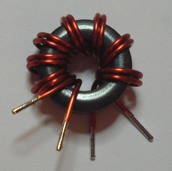
The T50-43 option, semi-finished transformer
To construct T1 and T2:
Cut two equal pieces of enameled wire of diameter about 0.3mm and length about 30cm.
Twist them together, not too tight (Note, even if you do not twist them they will work).
Wind 8 turns of this twisted wire on the toroid (A turn is made every time the wire is passed through the hole of the toroid).
Cut the remaining (unused) length of twisted wire and leave about 1cm or so, out of the toroid for the connections to be made.
Etch all the wires at their edges using a sharp knife.
With a multimeter find 1a, 2a, 1b, 2b as shown in the picture above (the beginning and the end of each wire) and mark them.
Solder 2a and 1b together. This is the output point of the buffer amplifier.
Point 1a is connected to the VCC.
Point 2b is connected to the transistor collector.
If one is to include the external crystal option he must use the schematic below. Relay RLY 1A and RLY 1B is a double relay (or two single ones activated together) and it is used to switch the crystal-capacitor combination between the transmitter and the receiver. It is activated by the CW key. SW1A and SW1B is a double switch and it is used to switch the crystal between internal and external one.
As mentioned above Nexus 6 includes a crystal oven and the construction of the oven must be done as noted in the relevant section. Do not get confused by the connection of the plus pole of the first operational amplifier to the ground. The plus pole is actually internally connected to a voltage reference and this reference is connected to pin 4, which is externally connected to the ground. Also, the case of the LM395 is connected to the emitter and the emitter is connected to the ground as shown on the schematic, so the transistor is directly screwed on the piece of aluminum and does not require any mica insulator. The LED indicates when the oven is switched on and it's change in brightness, indicates when the oven is just about to be switched on or off. When the oven temperature is stabilized, the brightness of the LED seems unchanged because the oven does not let the temperature to drop too much, such as to be detected by the LED.
Transmitter section up to the second buffer amplifier, including the crystal oven and the external crystal option
Now it is time for some testing of the transmitter chain up to this point using the oscilloscope. I have tested the oscillator first an then the system up to the first buffer amplifier and the results were very satisfying. When testing the oscillator and changing the crystals, I could always see a clean symmetrical sine wave on the oscilloscope. When the first buffer amplifier was added The sine wave was amplified and it still remained clean and undistorted.
I tested about 15 crystals through the HF bands and two of them seemed to cause the output of the first buffer amplifier clipping a bit at it's low end. It seems they provided too much power to the amplifier. I could correct this by altering the value of the frequency capacitor to about 25pF and then the sine wave was clean again but at a lower level. A very important note is that the frequency capacitor does not only change the frequency of the oscillator but it also changes the coupling between the oscillator and the first buffer amplifier and this means the output power of the oscillator. Since different crystals have different properties and the oscillator does not output the same power at all bands, I decided to leave the 50pF variable capacitor there and be more careful about it's tuning. I would start with a middle value of 25pF and slowly change the tuning upwards or downwards, but not too much, in order to avoid clipping with the more powerful crystals. As I said you should not shift the frequency of the crystal too much anyway. For ultra fine frequency adjustment (1-2Hz accuracy) you can slightly change the temperature of the crystal oven, when using the internal crystal option.
The output power up to the first power amplifier can be seen in the table below. As it is expected it is not constant throughout all the HF bands and this is mainly because of the oscillator/crystals, but it gives enough power to drive most power amplifiers. Linearity of the oscillator output power is not of much problem here because of the compensation method used later on.
| Frequency (MHz) | Oscillator multi-switch band | MAX Output power (Vpp) | ~ MAX Output power (mW) |
| 1 | 1 | 3.7 | 35 |
| 2.5 | 2 | 5.5 | 75 |
| 4.5 | 2 | 6.2 | 90 |
| 6 | 2 | 10.2 (clipping but corrected at 10) | 270 |
| 8 | 2 | 9.5 | 220 |
| 9 | 3 | 10.2 (clipping but corrected at 10) | 270 |
| 10 | 3 | 6.5 | 105 |
| 11 | 3 | 8 | 160 |
| 13 | 3 | 5 | 63 |
| 14 | 3 | 6.2 | 90 |
| 17 | 4 | 6.2 | 90 |
| 24 | 4 | 2.5 | 15 |
| 27 | 4 | 1.7 | 8 |
When added the second buffer amplifier to the transmitter chain, things were much different than expected. Lots of clipping at the lower end of the sine wave and very amplified high ends. In order to see an undistorted sine wave I had to reduce the driving power out of the first buffer amplifier too much. The undistorted class-A gain that I took out of this second buffer amplifier was very low and I decided that there is no reason to use this amplifier at all, so I have discarded it from the transmitter chain at this point of testing.
In order to raise the level of the output signal even more, I used another class-A buffer amplifier and I also made some improvements to the transmitter as far as concern the output power linearity throughout the HF bands. The improved schematic of the transmitter can be seen below.

I left T2 transformer unchanged and I used a 2N3553 transistor operating in class-A. This amplifier can deliver more than 150mW (8Vpp) output with only 1-2mW input. Since so low input power is needed, an attenuator network was added to avoid overdriving the amplifier. This attenuator network is also used to make the output power of the transmitter linear through the HF bands. It attenuates the input signal more when its level is higher and less when its level is lower. It is also needed for another reason, to provide a means of isolation between the two amplifiers and to reduce the unwanted harmonics of the signal. When you attenuate a high level signal and a much lower level signal by the same value of resistance, then both of the signals will be attenuated by the same amount. You see, a 1dB attenuation on a +20dBm main signal may not be of much importance but the same attenuation on a 0dBm unwanted harmonic signal is much more important. The attenuator network must be switched along with the capacitor network double switch, as shown in the schematic, so a triple switch must be better used.
The Values of the resistors in the attenuator network have been chosen to achieve a constant output power of 150mW (8Vpp). This was a "safe" level that let the second amplifier operate always in class-A. When inserting a resistor you also alter the impedance of the circuit at this point, but I found the simple resistor network to be satisfactory enough. As I explained earlier in the article, the 50pF capacitor can not only change the frequency of the oscillator but it also changes the output power (coupling) of the oscillator. This means that as you adjust the capacitor you also change the amount of signal that drives the second buffer amplifier. Even with the addition of the attenuator network, at some frequencies, the amplifier can be overdriven if the coupling capacitance is too high. Additionally, the output level of 8Vpp needs to be kept constant through the HF bands. Thus, careful tuning of this capacitor must be made when changing crystals.
A good starting point for the tuning of this capacitor would be to use a micrometer head on its shaft, like the ones used at the multi-turn potentiometers to count the turns. Then you can insert a crystal and alter the variable capacitor until you get an undistorted output signal of 8Vpp on the oscilloscope. Then write down the micrometric head reading. The next time you insert this crystal, you know exactly where you need to set the capacitor for an undistorted 8Vpp output signal, without using an oscilloscope. By using the capacitor in that way, you can not change the frequency of the oscillator using this capacitor anymore, because you will also change the output power. You could change the frequency of course, but you may get lower power output level or you may overdrive the second buffer amplifier. If you want to change the frequency of the oscillator without affecting it's output power level, it is better to use the crystal oven potentiometer and not the variable capacitor, therefore I have marked this capacitor as "power level capacitor" and not as "frequency tuning capacitor" anymore.
Since I have noticed a bit of distortion at the lower edges of the sinewave signal, I have decided to reduce the output power to 6-7Vpp by adjusting the power level capacitor. The sinewave is very symmetrical now from 1.6-30MHz. At 1MHz the sinewave seems not too symmetrical but you can still get the full output power, although a bit distorted. I have also made some additions to the circuit which can be seen below.
Combined with a coupler and a detector, a 200 microamperes DC current meter has been used to give an indication of the output power of the transmitter. This is useful for two reasons. Firstly, to see that the transmitter actually transmits and secondly, to ensure that the output waveform is undistorted as it should be. Using that meter in the configuration shown, you do not need an oscilloscope to monitor a clean sinewave output. I have done all the measurements and adjustment for you. Just insert a new crystal and adjust the power level capacitor so that the meter shows a value between 160-180 microamperes. This denotes a 6-7Vpp or 100-120mW undistorted output signal. The linearity of the coupler is good from 1.6-30MHz so the same setting applies for all these bands, but at 1MHz you have to adjust the meter to 120 microamperes and not to 160-180 microamperes. I have chosen a 3.6K resistor to limit the current of the meter to 180uA for full power, instead of 200uA to avoid having the meter saturated (and possibly destroyed) each time the transmitter transmits at full power.
T3, the coupler, is a transformer made of the same T37-43 core as T1 and T2. First wind 60 turns of 0.3mm diameter enameled wire. Then wind 6 turns of 0.3mm diameter enameled wire. Connect the 6 turns coil between the amplifier and the antenna. Then connect the 60 turns coil between the GND and the diode, as shown in the schematic.
The key envelope generator
The importance for a soft keying has been discussed in an article above. One way to achieve a soft keying envelope is to have a circuit that slowly varies the output power of your transmitter from almost zero to full power. This can be done by varying the supply voltage of the final amplifier or by attenuating the driving input signal to this amplifier. By experimenting, I have found that varying the voltage of the final amplifier to achieve a variable gain is not a good idea. At low voltages the sinewave became triangular and during sharp variations of the voltage, the amplifier was unstable.
It seems that the best solution for varying the input signal to the power amplifier is to use a variable resistor. We need a resistor that can be varied automatically so a light depended resistor (LDR) can be used. I prefer the use of LDRs because these are passive non-semiconductor elements and their effect should be the same as the effect of a variable resistor in the signal path. If you use an LDR, all you need to do is to control the brightness of a lamp, in order to achieve variable resistance. I have chosen to use a common high brightness white color LED as a lamp, which can produce very intense light using only a few volts, it lasts forever and it does not produce any heat. The LDR that was used was the VT43N1, which has a resistance of about 200K in complete darkness and its resistance drops to about 100-200 Ohm using the bright light of the white LED. You may use any other LDR but it is better to chose one that has great resistive difference between dark and light. Try to find one that has a resistance of 50-300 Ohm in full light. The specifications for the LDR that I used, noted a 2K resistance at full light but the testing proved that it can go down to 60 Ohms, so do not look only the specs, try it yourself. For the construction, use a small drilled pcb to have the LED and the LDR facing each other. Then use a thermally sink tube, a box or any other means, to isolate them from external lights. The construction should look something like the picture below. Note, it is better to first build and test the envelope generator circuit and then seal the variable attenuator, in order to notice the variations of the LED brightness and make any possible adjustments.
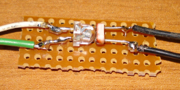
Construction of the variable attenuator
The LED driver (attack/release envelope generator) is the circuit that varies the brightness of the LED and hence the resistance of the LDR. I have tried many configurations including op-amps and transistors borrowed from audio envelope generators but none of them seemed to work satisfactorily enough for this purpose. It seems that the idea of the capacitor charging/discharging is the simplest effective approach that I was looking for. The envelope generator that I designed, charges a capacitor through a 2.2K resistor. During charging time, the voltage on the capacitor increases and the voltage across the LED increases too, so that the LED brightness increases slowly (attack). During discharging time, a resistor (1K potentiometer and 47 Ohms resistor) is connected at the circuit, in a voltage divider configuration as shown and the capacitor discharges both through this resistor and the LED (release). This approach is better than disconnecting the VCC and having the capacitor discharged only through the LED, because the discharging time of a big capacitor through a single LED is long, much longer than the charging time. This would lead to a very asymmetrical attack/release envelope generator.
My approach has also another advantage. A LED starts to light up when the voltage across its terminals is about 1V (this varies depended on the LED but let's assume 1V). Below 1V the LED cannot produce any light. From the other hand, the capacitor charging starts from 0V up to the maximum input voltage. This means that the LED connected across the fully discharged capacitor will not produce any light until the voltage on the capacitor exceeds 1V. In simple words this means that there will be a significant amount of time between the key press and the response of the transmitter to this key press, which is unacceptable for fast keying. In my approach, I keep a lower "maintaining" voltage to the capacitor even at key-off state, so that when I start to increase this voltage on key-on state, the LED immediately starts to light up, thus there is no time delay.
The operation is simple. The VCC is never disconnected from the circuit. Whenever I want to perform a "key press", I open RLY3 switch and the capacitor starts to get charged (remember the capacitor is never fully discharged). Whenever I want to perform a "key release", I close RLY3 switch and the capacitor starts to discharge through the LED and the resistor combination. To compensate for the different types of LEDs I have included a 1K potentiometer, which you must set for your type of led, until you notice an almost equal charging/discharging time. In my case, the potentiometer was set to 400K. I used two capacitors, which can be switched through a single switch, in order to achieve two options for the keyed envelope, a slow and a fast one.
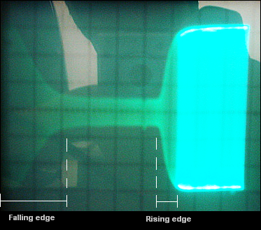
The fast envelope waveform
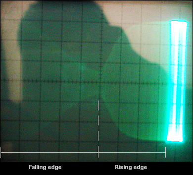
The slow envelope waveform
As you might have guessed, this type of key envelope generator never switches the transmitter completely off, it just varies its output power from a very low level to a very high one. It could be compared to the ASK (Amplitude Shift Keying) operation, having a great power difference between the "zeros" and "ones". The output power of the transmitter using this circuit, is 1Vpp (2.5mW) at "key-release" and 6Vpp (100mW) at "key-press". A third power amplifier that may be added to the circuit will not be able to be driven by such low input levels as 2.5mW, so at the antenna the "key-release" state will lead to zero output power. If you decide to use the NEXUS 6 without an external amplifier though, a 2.5mW output, plus the cable attenuation, won't let you transmit further than a few meters. Thus, the recipients won't be able to copy this very low "key-release" signal at all. Inside your lab, the transmitter will sound like a continuous signal was transmitted, even if you release the key. If you reduce the sensitivity of your receiver to minimum or add an extra attenuator, then you will be able to distinguish between on and off states of the transmitter, as you press and release the key.
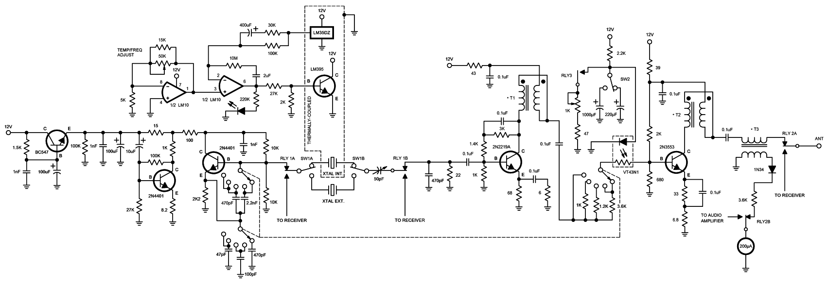
The transmitter schematic including the key envelope generator
The picture above shows the schematic of the transmitter including the key envelope generator. All the relays are shown in TX-mode state. The stability of the oscillator does not seem to be affected by the keyed operation, as I tried all the possible key combinations and I could not notice any frequency drift (1Hz accuracy), even at higher switching rates. The unused RLY2B switch, was used to switch the meter to the coupler during transmit and to the audio amplifier during receive operation.
There is a problem of using envelope generators though. Due to the envelope, when you release the key, the transmitter must be kept in TX mode until the release envelope sets the signal to its minimum power. But the relays do not follow the envelope generator, they just know two states, on or off. If we want the transceiver to automatically switch to receiver mode when there is no key-press, then we need a circuit that will be able to keep the relays activated, for as long as it needed for the key envelope circuit to finish it's work. Even better, the amount of delay of this circuit must be also directly related to the keying speed. For example, you do not want RLY1 and RLY2 to be toggled every time RLY3 is toggled. You just want to switch to receiver mode automatically, only when you have finished the whole transmission. It is not a good technique, to switch to receiver mode during spaces between words or letters because this introduces noise to the signal, produced by the relay contacts. Let's keep this noise limited only to the beginning and the end of the transmission and not during key-clicks. Thus, the time delay in which RLY1 and RLY2 must be kept on, is depended on the keying speed.
In NEXUS 6 there are two keying envelopes and thus, there must be two delay settings for RLY1 and RLY2. By the combination of two large electrolytic capacitors connected from the VCC of RLY1 and RLY2 to the ground and also the unused part of the double switch SW2, a suitable delay circuit can be made, that keeps these relays on until the capacitors are discharged. With the values shown in the next picture, the keying speed must be between 20-40 letters per minute (LPM) for the soft envelope and greater than 55 LPM for the sharp envelope setting. You could of course key at even slower speed than 20 LPM, but you will start to listen to the relay clicks between words or letters. Nevertheless, 20 LPM is a very slow rate, even for the starters in CW, but if QRSS is used, then there is no problem (apart from the key clicks that cannot easily heard at the receiver side due to noise levels in HF) of using even lower keying rates.
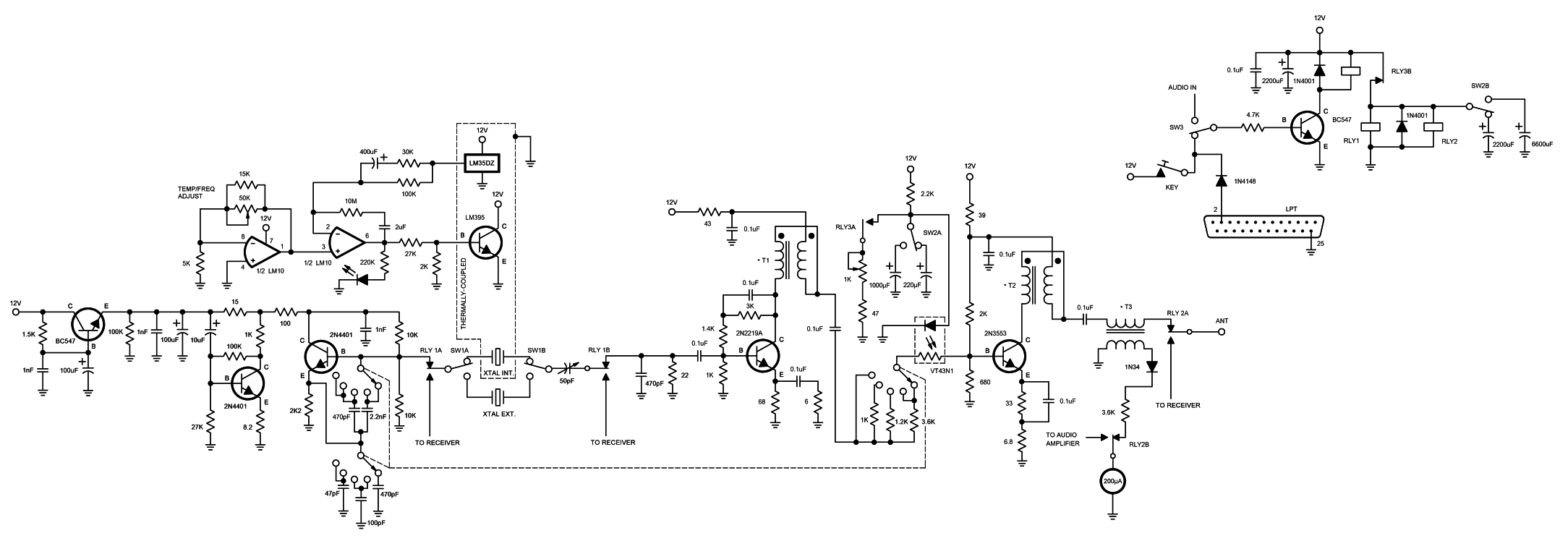
The transmitter including the control circuit
The transmitter control circuit is shown at the top right corner of the picture above. A transistor performs electronic keying to the transmitter and it keys RLY3, which in turn keys RLY1 and RLY2. We can now take apart the rest of the circuit and concentrate in controlling the transistor. There are three transmitter control option in NEXUS 6, manual control, computer control and audio control. Manual control refers to the standard morse code key, which passes 12V to the base of the transistor, through the limiter resistor. I have chosen to use the LPT port of the computer as an interface to the transmitter because I can control data bits easier than the serial port. For the keying, we need only one bit, so the first data pin of the LPT port was used. A 1N4148 diode protects the LPT port from accidentally pressing the manual key down and feed the LPT pin with 12V.
Many modern laptops do not have an LPT port (some of them not even a COM port) and rely on the USB ports to control everything. In my opinion, a computer without serial and parallel ports is unacceptable but it you already have one, I have included a circuit that controls the transmitter using the audio output of the sound blaster. Also, this has the advantage that you can use software that only outputs signal to the sound blaster and does not support the LPT port. The audio interface is capable of driving the transmitter from the line output of the computer at about half the audio volume setting of the sound blaster and above. I have tested all the audio tones from below 100Hz up to 3KHz and the interface works fine. The schematic of the transmitter including this circuit is shown below.
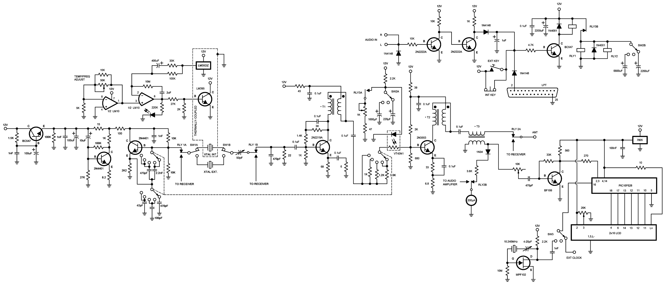
The transmitter including the sound control circuit
At this point I start to think of some essential improvements to the circuit. I had some near-by operators running morse code computer software. Whereas their ears could distinguish between different audio power levels, the computer software that they run could not distinguish the differences in the signal level introduced by the envelope generator, even if they lowered the sensitivity of their receivers at minimum. That is because the signal level transmitted in the zero-state of the transmitter was still too powerful for the near-by stations to distinguish it from the one-state. To cope with this, I had to add a circuit to switch off the envelope generator completely. The easiest way was to change SW2 with a DPDT ON-OFF-ON one. The middle position out of the three, disconnects the capacitors and therefore switches the envelope generator off.
When I go mobile, I do not want to carry the big and bulky key with me, so I added another key attached to the front panel of the transmitter in a place that I could easily access. It is just a momentary switch that is connected in parallel to the external key socket. Of course you could not expect the same settings and convenience like the external key but it is small, lightweight and attached on the transmitter.
If you go for such narrow bandwidth, you must have an accurate frequency counter to measure the frequency variations. The accuracy must be in the order of 1Hz. Most commercial and home brown counters have 10Hz accuracy. This is just not suitable for such low bandwidths. On the other hand, the counter used in NEXUS 6 must be small, cheap and simple to make. Even though I try to avoid using microcontrollers, it seems that the microcontroller offers the most in this application, as it provides both the accurate counting and the display driving mechanisms in a very low component count configuration. I have chosen the counter that can be found here (web copy here), which is ultra simple and offers 1Hz accuracy. It uses the well known and easy to find PIC16F628. I had to make some modifications on the counter though, to suit the project needs. The microcontroller can be easily programmed using one of the many home brew programmers available on the internet, but if you cannot program it yourself I will be happy to program it for you.
If you want the counter to be stable, you must provide it with a stable reference frequency. The variations in the frequency of the crystal due to temperature changes, lead to an unstable clock, so I had to add an option for a connection of a stable external clock. I had to modify the assembly code a bit to use only pin 16 of the PIC as a clock input and leave pin 15 unconnected. To use the internal clock now, you have to add an oscillator circuit. Signal quality is not important here, so I made a quick and dirty oscillator using low-count components. A BNC connector and a DPDT ON-OFF-ON switch was added at the back of the transmitter, which allows to chose between internal and external clock. The middle position of the switch disconnects the clock from the PIC completely. This has the effect that the display freezes at the last read frequency. This can be very useful and adds a last-read-frequency memory-like operation to the transmitter. The modified program for the counter can be found here.
The 1 second gate time of the counter gives a precision of 1Hz, which is what is needed. The counter needs 3 seconds to read the exact frequency so if the keying speed is fast it will not be able to read the correct frequency. So the best thing is to press the key for 3 seconds, read the frequency and then if you want disconnect the clock, using the rear switch, to remember at what frequency you transmit. Alternatively, don't bother reading the frequency during fast keying. The display used is a standard 2x16 LCD display found easily in many electronics shops. This has 14 pins and if it is back-light enabled it has two more pins for the back-light. Eventually, I realized that it was difficult to read the LCD in bright light, or when looking by the sides. The refresh rate and the contrast of the LCD is also low, so I have decided to replace it with a compatible organic led (OLED) display which, among it's advantages, gave a more professional look to the transmitter. When measuring the frequency, I found that during gate times the signal moved a bit on the oscilloscope screen. The front panel power meter also gave much lower readings. This was due to bad isolation and too much RF power sucking I guess, so I added a 10K potentiometer at the input of the counter and set it about 8.2K to solve this problem.
The transmitter including the modifications and the counter
The power amplifier
Now that we have a modest power out of the buffer amplifier, it is time to make the next stage, the power amplifier. Consider the parameters that I have mentioned above, when choosing between class-A and other classes of operation for the final amplifier. Currently, I have found the next very interesting application notes:
BLF175 for about 8W of output power (including the PCB pattern).
BLF244 for about 4W of output power.
These are broadband amplifiers that operate in pure class-A. They can be used as final amplifiers, or as drivers, to drive bigger final amplifiers. These are really good designs and I recommend them. The only thing I do not like is the toxic beryllium oxide base, used in these devices so please read the precautions when using such devices. Personally I do not like playing around with toxic or radioactive materials in my lab, but if the transistor is not broken, you are entirely safe. I used to use such transistors at the past without even knowing how toxic they can be if they are broken. I never had the chance to see one of these inside, but hopefully an Italian amateur has opened a faulty MRF422, which is quite similar to them (I would never try this at home!).
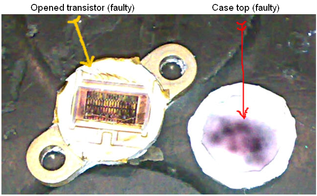
Faulty MRF422 transistor opened (similar to BLF175)
Another disadvantage of these transistors is that they are very expensive and quite obsolete, especially the BLF175. I managed to find the BLF175 for $75 and I think this is too expensive for a homebrew project. Also, the designs provided, operate using a 50V power supply which is not too convenient. On the other hand, the BLF175 broadband amplifier can amplify a few mW (~13mW) to 8W in single ended class-A operation, using a 50V power supply and no complex output transformers (I almost always prefer single ended designs, both in audio and in radio amplifiers when high quality is needed, because of the complete absence of cross-over distortion). Also, the increased output power of 8 watt is capable of driving most class-AB power amplifiers up to 300W, if this amplifier is to be used as a driver for a more powerful transmitter. The BLF175 application note includes the PCB pattern but I am pretty sure that this can apply to the BLF244 too (not checked in detail).
An alternative solution would be this article that I have found in a German magazine. I do not think this is a class-A amplifier (I have to test it on the oscilloscope) but it is well designed and it is linear. Note, the article was really messy and it took me 2 days to re-organize it in order to translate it using on-line automatic translators, so please do not judge the bad English translation. It should provide you with the necessary information to build it. I have to say, I found great difficulty in finding the 25 Ohm coaxial cable needed for the output transformer, these are quite obsolete.
Another class-A option would be this document that uses a BLX15, but the schematic provided is for 27MHz, so a little bit of testing would be needed to ensure that it will work ok down to 1.6MHz.
A very interesting approach is this one. This is not a class-A amplifier but I do not see a reason why it couldn't be biased in class-A. Furthermore it uses 4:1 easy to build transformers and it is quite broadband. The most important thing is that it uses cheap CB transistors that can be found from older CBs. I also found spares for $4 each. Now compare this to the $70-$80 of an obsolete transistor, if you burn one, no problem, you can easily replace it. If you burn a $75 transistor it's a disaster and transistors like BLF175 are difficult to de-solder without braking them (and get contaminated). The transistors used on this design are also BJT devices, which I generally prefer, that are designed from Mitsubishi for actual RF amplifiers and not just for switching applications (like IRF510 mosfet).
Since the cost is an important issue in NEXUS 6, I have decided to try the fourth design for the power amplifier and make some modifications on it. Currently, I have made some modifications on the biasing of this amplifier and I have managed to make the first stage work in class-A from 4-30MHz but I will post the complete schematic below, as long as I complete the construction.
At this point I had to make a decision, whether to include this amplifier in the QRP transmitter box or to make it in a separate box. I have found the leakage from this power amplifier to alter the operation of the crystal oven op-amp. This can be solved by using coaxial cables for the inter-connections of the RF signals and some shielding between stages, but since I was running out of space in the small box and since this amplifier required more band-switching and heat sinking, I preferred to make it in a separate box. This has also another advantage, if you decide that you want to change the power amplifier with another one, you have to just unplug it from the connector and you do not need to de-solder components. The disadvantage is that you have to carry two boxes (for mobile operation) and you also have to have more power cables, one set for the transmitter and one for the power amplifier.
To overcome the second problem I have decided to use the "phantom" power supply technique, that is widely used in television amplifier systems. The power and the signal of the amplifier are both passed through the coaxial cable. I have to test though if and how this may affect the sinusoidal signal.
TO BE CONTINUED...