by SV3ORA
original idea by
SM0VPO
In this page I have borrowed all the information from the website of SM0VPO and I have added my technique and other information to make a complete guide of how to construct any inductance coil printed on PCB.
It is a fact that if 10 different people wind a coil according to the same instruction, you will have 10 different coils. You may also see people asking for things like wire thickness, insulation material, turns spacing, and even temperature. Not may think about the mood, thinking processes or patience of the winder, but these have a far greater impact upon the final coil produced.
Now there is a solution to this. Etch the coils on a PCB. These coils that are constructed (printed) on a PCB just like you print your circuit lines on a PCB. This technique is widely known on UHF and microwaves, where the coil sizes must be made compact and the inductances accurate and relatively low. For coils of a higher inductance, a multi-layer PCB may be required. So here it is:
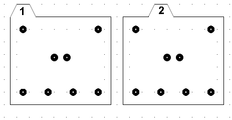
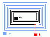
Harry says, I fitted wires to the receiver PCB so that there was about 3cm of wire sticking up from the board on the component side of the PCB. Onto these I fitted in turn, four boards, each with a spiral coil. The receiver PCB must have the same coil pin spacing and all coil PCBs must be made from the same template. Here is the blank template I used:
The pads and their spacing can then be copied to the main project PCB for perfect spacing of the wires. To each of the above PCB I added a spiral track to form the inductor. Note that alternate boards must have the spiral in the opposite direction. Because there are three centre transition-pads, there can be a maximum of 6-layers with this example, but you can add many more, as you see fit. If you use Harry's PCB tracks and pads (Download them here) to create PCB's then the scale of this project will fit nicely. Here is an example of the first prototype PCB coil foil pattern, but here only two of the four layers is shown:
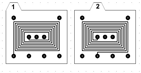
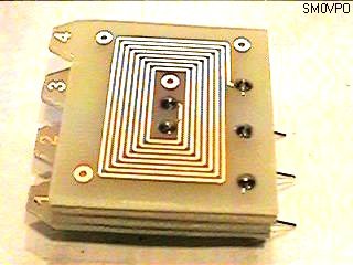
Each board is 35mm x 40mm (excluding the order tabs) and has sufficient room for 9-turns. With the design above I achieved 4-layers, each having an inductance of 5uH. the four layers therefore gave me 20uH so they can be brought to resonance at 4MHz with just 150pf. With four layers I also had three tapping points, 25%, 50% and 75% of the coil, all of which can be accessed on the project from any direction board without links or tracks crossing. Here is a photograph of the first prototype PCB coil. I built four of them and all were within 1% of each other's inductance.
I see no reason why the coil assembly cannot have the wire leads projecting from both sides of the boards and the coil then mounted verticall on the PCB. If you want to be really clever then you could have plug-in coils with the in-built padding capacitors for tuning.
The PCB coils have high precision (about 1%) and thus you can produce matched pairs, quads etc. Another advantage is the rigidity. They cannot be bend or distort. Also, if desired, complex shapes can be produced, that couldn't be produced by air core wires before. A disadvantage could be the bigger size, when talking about higher inductances, but the multilayer approach shown above can solve this.
There are a few software tools that could help you make your own PCB coils from scratch, like Sonnet and the DOS version of APPCAD (restricted to 1nH max inductance). There are also spiral coil shapes and other ones but I will stick with square ones because I believe they fit very well to PCBs and saving space.
Now I will show you a way to construct coils of this type with any inductance value you like. It is simple as this:
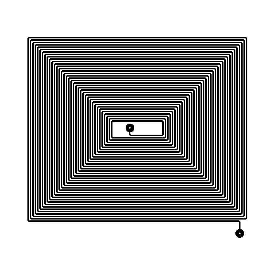
A multi meter capable of measuring inductance is required. Starting with a predefined pattern and with a trial and error measurement, you can find your desired coil value. Lets try the procedure step by step:
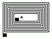
Print the pattern on a PCB.
When printed, switch your multi meter to inductance and connect one pole to point A.
With the one pole connected to point A, connect the other pole of the multi meter to different points across the coil lines and measure the inductance at each point.
When you achieve the desired inductance, mark this point with a marker.
Lets say you have found the desired inductance in point B. Cut the PCB trace at this point with a cutter, in order to isolate the desired coil from the undesired one. This is not mandatory but it will be better to do so. If you do not cut the coil at this point then you may desire to have a multi tap coil (taps A, B, C). You can connect as many taps as you like, just like ordinary coils.
If you do not want a multi tap coil, then cut the trace as mentioned above and connect a lead wire from the points A and B of the coil, to your circuit and leave the rest of the coil unused or..
You can cut the PCB carefully around the wanted coil, in order to keep only this part (and reduce the size of the coil).
By this trial and error process you can make all your coils. If you make a coil with a desired inductance once, then keep the record, so you do not have to do the same process all over again. Instead of starting with an arbitrary pattern, another good option would be to use Harry's pattern as a starting point for a single layer, because you know that each layer has an inductance of 5uH.
If you want 5uH just print Harry's pattern.
If you want less than 5uH, print Harry's pattern and then follow my process to achieve the desired inductance.
If you want more than 5uH, for example 13uH, then you can do two things:
You can print Harry's patterns 1, 2 and 3. Patterns 1 and 2 will make 10uH, so you need only 3uH more from pattern 3 in order to reach 13uH in total. Then follow my process for the 3rd pattern only, to achieve the desired inductance of 3uH. When done, connect patterns 1, 2 and 3 together.
Alternatively (and if the size permits it), you can start by an arbitrary pattern like I have shown you above, and make only a bigger single layer coil. In order to make the job easier I have made a bigger pcb coil pattern which you can find here.
An important note here. The parameters that define inductance in a PCB coil is a combination of the width of the pattern lines, the space between turns, the number of turns, the thickness of the pattern lines and the use of ground plane below the coil or not. So this is quite complex and that is the reason I suggest you this trial and error procedure, unless you have (and know how to use) a PCB coil design software. My guess (I have not tested this) is that if more power needs to pass through the coil then you should make the width of the lines bigger and maybe the spacing between them bigger to prevent arcing. I do not know how much power can Harry's coil handle, but for oscillators and low power circuits it should be fine.